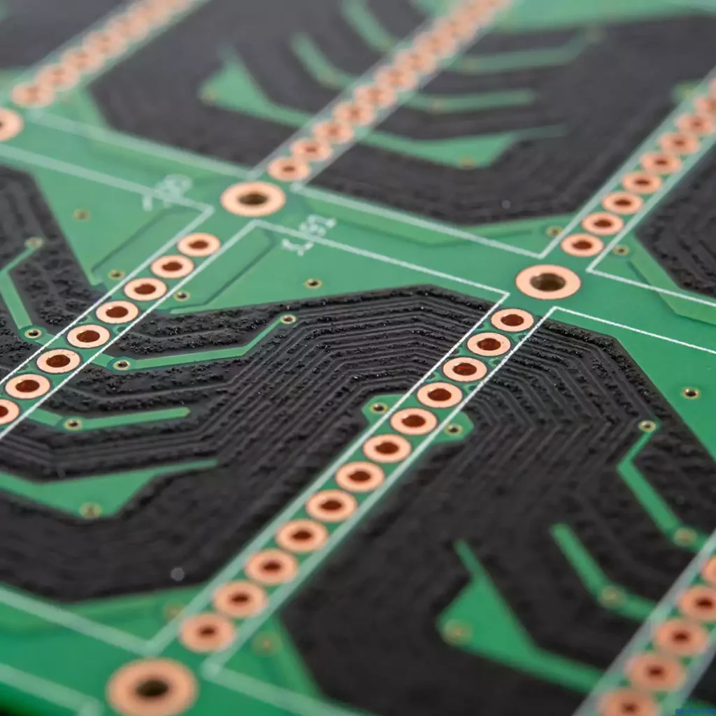
First of all, Carbon Ink PCB (also known as carbon ink printed circuit board) is a specialized PCB that uses screen-printed carbon ink as a surface treatment process. This common surface treatment is widely applied to single-sided and double-sided Printed Circuit Board(PCB). Using screen printing technology, manufacturers apply carbon ink to specified positions on the board. After oven curing and testing, the carbon ink forms a conductive carbon film with a specific resistance value, which can replace traditional discrete resistors in the circuit. The production process is similar to screen printing, and carbon ink offers excellent conductive properties for electronic applications.
1. Composition of Carbon Ink
Furthermore, carbon ink is a composite material with three main components, each serving a critical function:
- Synthetic resin: Acts as a binder (carrier) to hold the ink together and adhere it to the PCB surface.
- Hardener: Triggers the curing process, ensuring the ink solidifies into a durable, stable film.
- Carbon powder: Provides the core conductive properties. Some manufacturers may add graphite powder for enhanced conductivity, though this increases production costs. To achieve lower resistance and higher conductivity, some suppliers also mix a small amount of silver ink into the carbon ink formulation.
2. Carbon Ink PCB Production Capacity
In addition, carbon ink PCB fabrication requires strict control over design and manufacturing parameters to ensure performance and reliability. Key production capacity specifications include:
(1) Carbon Ink Gap Requirements
Notably, carbon ink has excellent conductive properties, so finished boards require specific gaps between carbon ink traces to prevent short circuits. For standard production:
- Minimum finished gap: 8mil (for ½ oz bottom copper)
- Minimum finished gap: 12mil (for 1–3 oz bottom copper)
To minimize short-circuit risks, designers should increase gaps whenever possible, especially when using film-based production processes.
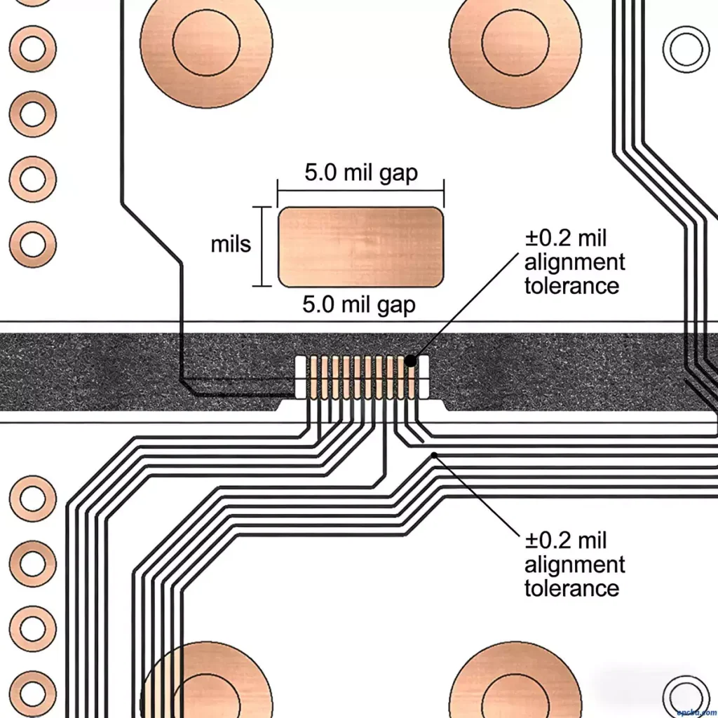
(2) Minimum Alignment Tolerance
Moreover, carbon ink printing has a minimum alignment tolerance of ±6mil. To account for alignment errors and ink seepage:
- Carbon ink pads must extend at least 6mil beyond copper pads (½ oz bottom copper) or 8mil (1–3 oz bottom copper) to avoid exposed copper.
- Carbon ink windows must maintain a 6mil (½ oz) or 8mil (1–3 oz) gap from surrounding copper patterns to prevent short circuits caused by ink coverage.
(3) Carbon Ink Thickness
Additionally, carbon ink thickness directly impacts resistance and conductivity. Standard specifications include:
- Single screen print: 0.3–1.0mil, with a thickness tolerance of ±0.3mil.
- For thicknesses ≥1.0mil, a second re-print is required, resulting in a total thickness of 1.0–2.0mil and a tolerance of ±0.4mil.
- The second re-print carbon ink film must be 3mil smaller per side than the first print, requiring two separate tool sets in the manufacturing instructions (MI).
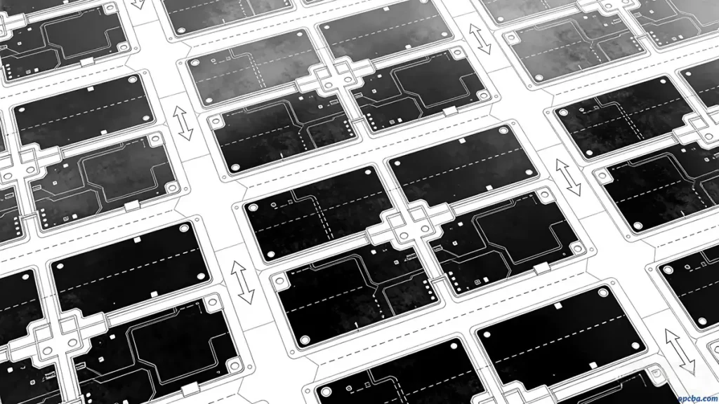
(4) Panelization Guidelines
Finally, panel design is critical for efficient carbon ink PCB production:
- Preferred production size: ≤16″ × 18″ for optimal screen printing control.
- If larger panels are needed (due to material utilization), manufacturers must cut the panel after the white solder mask process (before carbon ink printing). This requires clear notes on the LOT-CARD in the MI and careful design of cut lines.
- When designing panels, align carbon ink printing directions to simplify production control and ensure consistent quality.
3. Key Design & Manufacturing Notes
Furthermore, several critical considerations ensure the reliability of carbon ink PCBs:
- Surface treatment compatibility: Boards with immersion silver or immersion tin surface treatments should not be printed with carbon ink directly. These surface treatments are prone to oxidation, and carbon ink printing can scratch the surface. Instead, manufacturers must print carbon ink first, then apply immersion silver or tin—note that the carbon ink area will also be coated during these processes.
- Key shrinkage: Original boards with integrated keys must undergo shrinkage treatment to maintain dimensional stability.
- Baking temperature control: Oven curing temperatures must be gradually increased from low to high to avoid thermal stress and ink cracking.
- Ink dilution: Carbon ink must be diluted strictly according to the manufacturer’s specifications to ensure proper viscosity and print quality.
For professional carbon ink PCB fabrication services that meet these strict standards, you can contact our experts at opcba.com to start your project.


