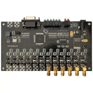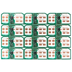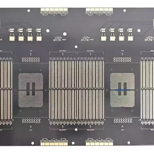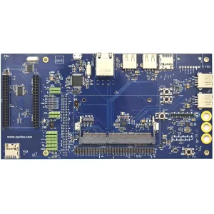
Overview of Network equipment PCBA
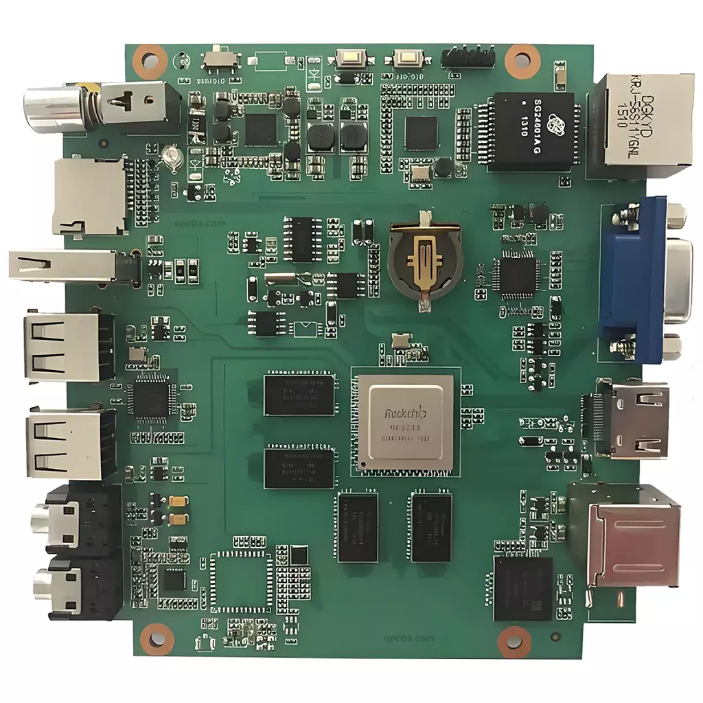
Network equipment PCBA is a functional unit completed after the welding, assembly and testing of components on the basis of a PCB. A finished assembly brings together the bare board, active and passive components, connectors and soldering materials, and the way those parts are joined is what decides how the equipment behaves in service. Boards in this category sit inside switches, routers, base stations and optical transmission equipment that are expected to keep running without interruption.
What network equipment boards demand from a build
1. Impedance discipline: the SerDes pairs behind 10G, 25G and 100G ports are routed as 100 ohm differential lines, so even a small impedance excursion turns into reflection and lost link margin.
2. Layer count and via stubs: core switch and backbone router backplanes commonly run 16 layers and above, where every unused via barrel below the signal layer acts as a stub that resonates at high frequency. Back drilling is the standard answer.
3. Laminate loss: insertion loss on standard FR-4 climbs quickly with frequency, so long high speed runs are usually built on low loss laminates or on a hybrid stack that pairs FR-4 with high frequency material.
4. Heat and uptime: network processors concentrate a lot of power in a small area while the equipment runs continuously, so thermal pads, thermal vias and interface materials matter as much as the routing.
How our process covers it
Rigid boards run from 1 to 70 layers, which covers the high layer count backplanes this category needs, and HDI is available at 1+N+1, 2+N+2 and 3+N+3. Outer layer trace and space go to 3 mil on 18 um base copper, and laser drilling reaches 0.10 mm. Impedance is designed into the stack up rather than corrected after etching, held to +/-5 ohm for targets under 50 ohm and to +/-10 percent at or above 50 ohm. For loss sensitive runs we process Rogers and Taconic materials alongside standard FR-4, and the finished board can be tested on flying probe or universal grid equipment before it ships. If the project also covers server class hardware, see our AI server circuit board page, and high speed PCB goes deeper into the routing side. Figures above are typical values from our capability sheet.
Core Production Process of Network equipment PCBA (8-stage Simplification)
1. PCB Incoming Inspection (IQC): Screening for quality issues such as PCB circuits, hole diameters, and surface conditions.
2. Incoming Inspection and Material Preparation of Components: Verifying model parameters, categorizing and preparing materials to avoid wrong or damaged materials.
3. Solder Paste Printing: Uniformly applying solder paste on PCB pads, controlling thickness and accuracy.
4. SMT Assembly: Precisely placing components onto pads, controlling assembly accuracy.
5. Reflow Soldering: Melting solder paste at high temperature to achieve secure connection between components and PCB.
6. DIP Insertion Welding (as needed): Hand or automated insertion welding of components to ensure firm connection without short circuits.
7. Cleaning and Repair: Removing residual impurities and repairing short circuits, loose soldering, and similar defects.
8. Finished Product Inspection (FQC) and Packaging: Inspecting appearance and functionality, then packing for anti-static and moisture-proof delivery.
Two of these stages carry more weight on a network board than on most others. Impedance verification at incoming inspection catches a stack up that drifted before any component is placed, and functional test at the end separates a board that merely has continuity from one that still holds link margin at temperature.