Lead-free PCBA processing refers to manufacturing PCBs without lead at any production stage. In recent years, RoHS-compliant PCBA assembly has also drawn significant attention in the electronics industry. Traditionally, lead was used in PCB soldering. But lead is toxic and harmful to human health. For this reason, the EU’s Restriction of Hazardous Substances (RoHS) Directive bans lead in PCBA manufacturing. In fact, the shift toward environmentally friendly PCBA production has become industry standard worldwide.
Replacing lead with low-toxicity materials barely changes the PCBA workflow. This guide breaks down the Lead-Free PCBA processing process step by step, aligned with industry standards.

RoHS-Compliant PCBA Core Guidelines
The Lead-Free PCBA workflow splits into two phases: pre-assembly preparation and active assembly. Each phase follows strict RoHS and IPC standards to ensure safety and reliability, highlighting the importance of best practices in lead-free PCB assembly.
RoHS-Compliant PCBA Pre-Assembly Preparation
These steps lay the foundation for error-free, precise Lead-Free PCBA assembly. They ensure compatibility and quality before production begins, which is critical for thorough environmentally friendly PCBA manufacturing.
Prototype & Compatibility Analysis
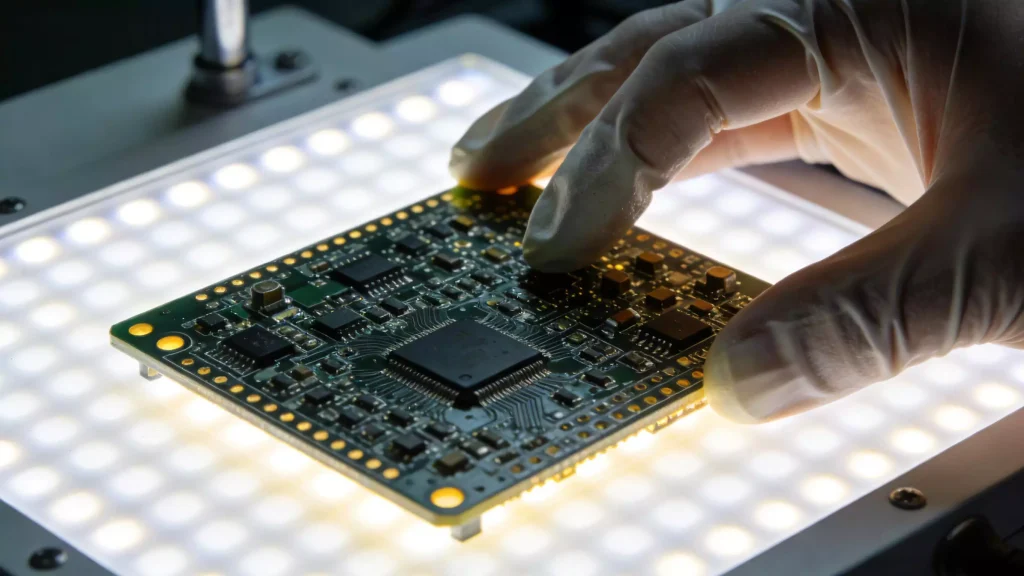
Manufacturers use a functional or dummy PCB as a prototype. They compare lead-free component designs to the prototype to confirm fit. Contour tracking ensures the assembly template matches the PCB layout. This step eliminates compatibility risks early.
Solder Paste Inspection
RoHS-compliant PCB solder joints have a distinct metallic appearance, different from lead-based alternatives. Inspectors check PCB shape and solder paste against the IPC-610D standard to ensure strong, durable joints. They also test moisture levels—lead-free soldering exposes boards to higher humidity than traditional methods, further emphasizing the rigors of modern environmentally friendly PCBA production.
BOM & Component Validation
Customers must verify their Bill of Materials (BOM) to confirm all components are suitable for Lead-Free PCBA. Lead-free components are moisture-sensitive, so manufacturers bake them in an oven to remove excess moisture. Once validated, the active RoHS-compliant PCBA assembly phase begins.
RoHS-Compliant PCBA Active Assembly Workflow
This phase executes the physical Lead-Free PCBA assembly, following lead-free and RoHS-compliant practices to maintain processing that is entirely lead-free.
Stencil Placement & Solder Paste Application
A precision lead-free stencil is placed over the PCB. Lead-free solder paste (typically SAC305 alloy) is applied through the stencil to create uniform solder deposits. This ensures consistent joint quality for SMT components, which forms part of the broader lead-free PCB assembly approach.
Component Placement
Components are placed onto the solder paste—either manually or via automated pick-and-place machines, which rely on high-speed SMT placement equipment (learn more about market trends in our 2026 Global High-Speed SMT Equipment Market Analysis). All parts are pre-validated in the BOM phase to ensure Lead-Free PCBA compliance.
Lead-Free Soldering
Soldering is performed using lead-free materials, whether for through-hole (THT) or surface-mount (SMT) components. This step adheres to ANSI/J-STD-001 lead-free soldering standards to ensure joint integrity, supporting high reliability in environmentally friendly PCBA manufacturing.
Reflow Oven Processing
RoHS-compliant PCBs require high temperatures to melt solder paste evenly. The PCB is placed in a reflow oven, where controlled heating melts the paste. After heating, the board cools at room temperature to cure the solder, locking components in place.
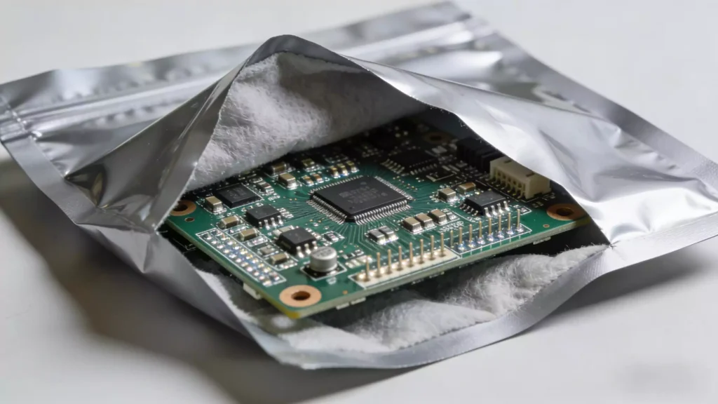
Testing & Anti-Static Packaging
PCBs are tested against the IPC-600D standard to validate performance. Inspections include visual checks, AOI (Automated Optical Inspection), and X-ray analysis of lead-free PCB solder joints. Physical and functional tests confirm reliability before packaging. For shipping, PCB is sealed in anti-static discharge bags. This prevents static damage during transportation, protecting the finished Lead-Free PCBA before it completes the final steps of environmentally friendly PCBA production.
Even with a clear grasp of Lead-Free PCBA processing, expert input is key to refining results. As a one-stop PCB service manufacturer, opcba.com specializes in lead-free PCB manufacturing. We use RoHS-compliant FR4 materials and follow IPC-A-600D and ANSI/J-STD-001 standards for every project. Our end-to-end services ensure your PCBs meet global safety and quality requirements, from design optimization to mass production by strictly applying Lead-Free PCBA expertise.