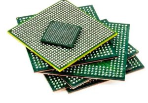
Why BGA Packaging Enables Device Miniaturization? Types and Core Advantages
BGA packaging, short for Ball Grid Array packaging, is an integrated circuit packaging technology in which the I/O terminals are arranged in […]
BGA packaging, short for Ball Grid Array packaging, is an integrated circuit packaging technology in which the I/O terminals are arranged in […]
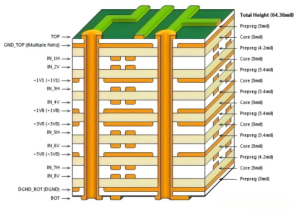
What is a PCB stackup? A PCB stackup refers to the arrangement of copper layers and insulating layers that make up a
Most board failures I’ve traced over the years didn’t come from faulty components. They came from subtle layout decisions made in the
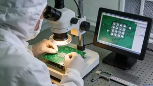
Electronic Manufacturing is a critical partner for tech companies looking to streamline product development and manufacturing. Opcba’s ODM/EMS service delivers end-to-end support,
If you’ve ever stared at a dense BGA breakout and wondered whether you could squeeze two traces between pads without blowing the

Robot PCBA is the core electronic control unit for robotic automation systems. It powers the brain of Industrial Control, collaborative, and service
PCBA testing is a critical quality control practice in Electronic Manufacturing(EMS), ensuring that PCB Assembly(PCBA) meets design specifications and perform reliably in
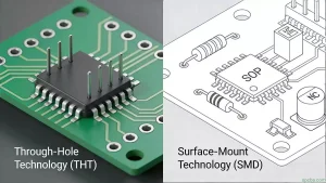
Electronic component packaging is a critical foundation of reliable PCB design, directly impacting performance, thermal management, and manufacturing efficiency. As semiconductor technology
sales@opcba.com