Imagine a slim smartphone handling crystal-clear calls worldwide. Or a remote IoT sensor sending data perfectly in tough conditions. The circuit board makes this possible in every communication device. As a PCB manufacturer specializing in communication devices, we see daily how smart circuit board design turns wireless communication technology into reliable performance. This guide explores PCBs in communication devices. It covers core principles, real manufacturing facts, and future trends.
The Foundation: Why Circuit Board Design Defines Communication Device Reliability
Communication devices include base stations, routers, satellite terminals, wearables, and industrial gateways. Each communication device relies on its PCB for fast signals, low losses, and steady synchronization. Unlike basic consumer products, communication devices need PCBs built for tough environments. They must handle interference, temperature swings, and high frequencies.
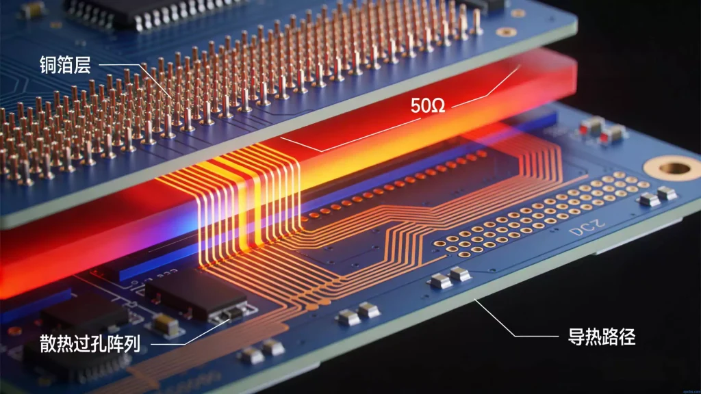
Modern wireless communication technology uses microwave and millimeter-wave bands. A bad trace can cause reflections or crosstalk. This raises bit error rates too high. Good circuit board design starts with controlled impedance. We target 50 Ω single-ended or 100 Ω differential lines. This needs exact trace width, spacing, and copper thickness.
Thermal issues are critical too. Power amplifiers in 5G communication modules create hot spots. Heat shifts material properties and causes drift. For example, add thermal vias and heavy copper pours. Use embedded heat spreaders when required. In communication device projects, microvia thermal networks reduce heat by up to 35%. This outperforms standard FR-4 boards.
Material Selection: Balancing Performance, Cost, and Manufacturability in PCB Manufacturing for Communication Devices
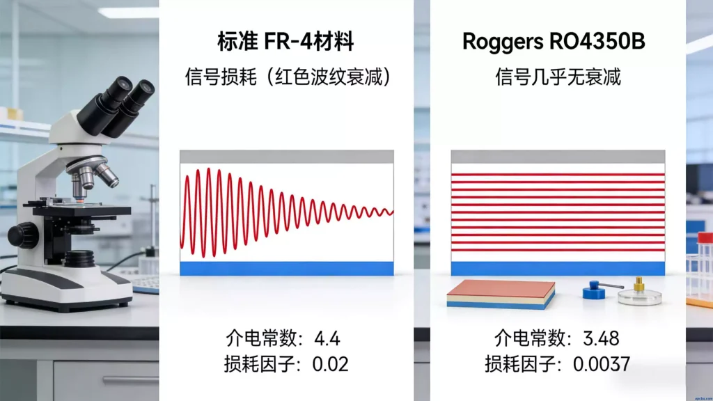
Substrate choice shapes RF performance and cost for communication devices. FR-4 works well for sub-6 GHz bands. However, it loses too much signal above that. Its loss tangent reaches 0.015–0.020 at 5 GHz. For mmWave 5G communication modules (24–52 GHz), low-loss materials become essential in communication devices.
Popular options include:
- Rogers RO4350B and RO4835. They offer Df ≈ 0.0037 at 10 GHz. They provide stable expansion for base station units. Explore why Rogers materials excel in high-end applications in our dedicated post: [Rogers Laminate – The Optimal Solution for High-End Communication Devices]
- Isola Astra MT77. It has Df < 0.0018. It excels in phased-array antennas for communication devices.
- Taconic RF-35. It gives good peel strength at lower cost.
Hybrid builds save money in communication devices. Use low-loss material for RF paths. Then add FR-4 for digital layers. Blind and buried vias connect them. This reduces material costs by 20–40%. It still keeps RF quality high.
Surface finishes matter as well. Immersion silver provides great conductivity. Yet it risks tarnishing in humidity. ENIG resists corrosion better. It supports wire bonding. For most 5G communication module projects in communication devices, ENEPIG offers the best balance of performance and reliability.
High-Frequency Layout Techniques for Superior Signal Integrity in Communication Devices
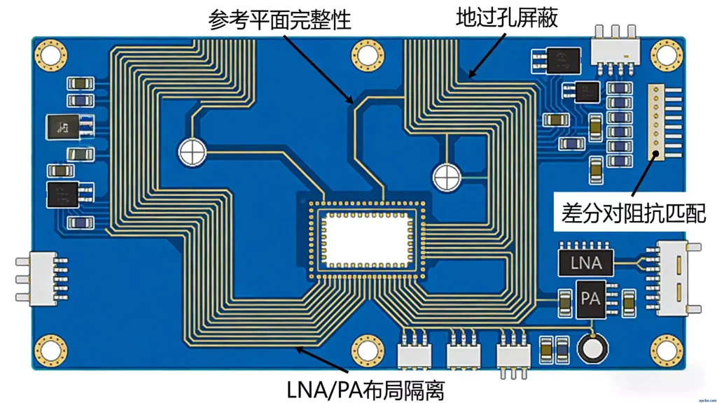
Low loss and high return loss require careful layout in communication devices. Start with solid reference planes. Avoid splits under fast traces. Instead, use full copper pours. Stitch them with vias every λ/20 distance. In multilayer boards, dedicate layers to ground or power. This lowers inductance significantly.
Vias can limit performance. Back-drill unused stubs to stop resonances. Above 20 GHz, shield signal vias with ground rings. This cuts crosstalk by 10–15 dB.
Length matching is strict. Differential pairs for PCIe need ±0.5 mil skew or less. Serpentine tuning avoids sharp corners. These prevent impedance jumps in communication devices.
Place RF parts first. Put LNAs, PAs, and filters near antennas. This shortens lossy paths. Keep digital chips and power supplies separate. This limits EMI in every communication device.For detailed layout guidelines, refer to our [Printed Circuit Board cornerstone post]
Power Integrity and Decoupling Strategies in Modern Communication Devices
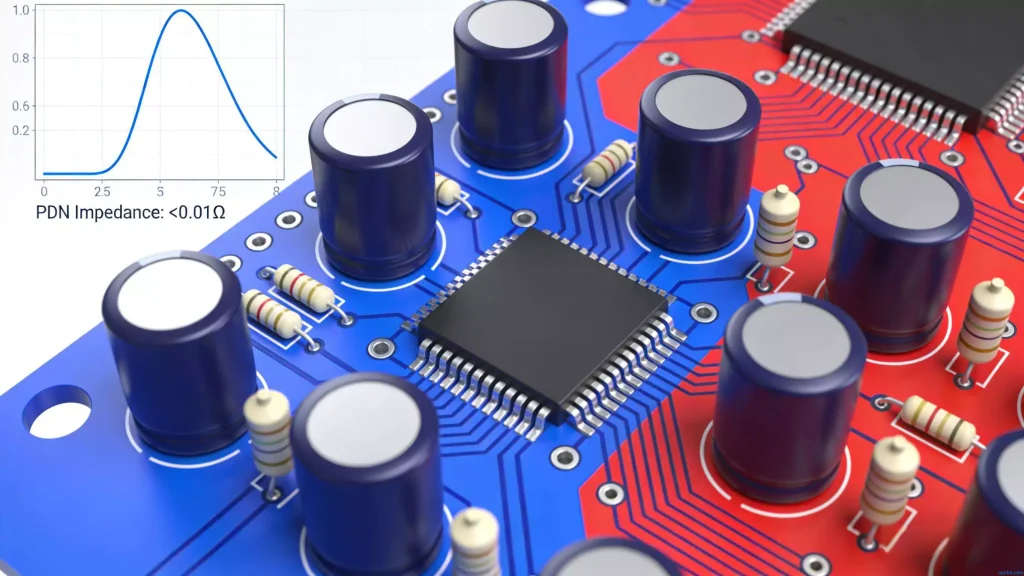
Communication devices use multiple voltages. Examples include 1.0 V for logic and variable Vcc for amplifiers. Small ripple (10 mV) can harm oscillators or add noise.
Decoupling combines large capacitors (10–100 µF) with small ceramics (0.1–1 µF). Place ceramics next to pins. In mmWave areas, use via-in-pad for low inductance.
Analyze PDN impedance. Keep it under 0.01 Ω from DC to GHz. This prevents noise peaks. As a result, high modulations remain clean in communication devices.
Advancements in 5G Communication Module PCB Technology for Next-Gen Communication Devices
5G communication modules demand dense designs. They include MIMO arrays and beamforming. PCBs must fit antennas, RF chains, and fast interfaces together in communication devices.
Phased arrays need matched lengths. This keeps phase accurate. Use 8–16 layer HDI with microvias. These provide routing space for communication devices.
Warpage control is key during soldering. Low-CTE cores and balanced copper help. They ensure good BGA joints.
Embedded components reduce parasitics. Bury passives or small ICs. This shortens paths. It improves EVM for 256-QAM and higher in communication devices.
Manufacturing Considerations: From Prototype to Volume Production of Communication Device PCBs
Move from prototype to volume smoothly with DFM early. Panel setup, fiducials, and test points affect yield for communication device PCBs. Add impedance coupons on panels. This verifies every lot.
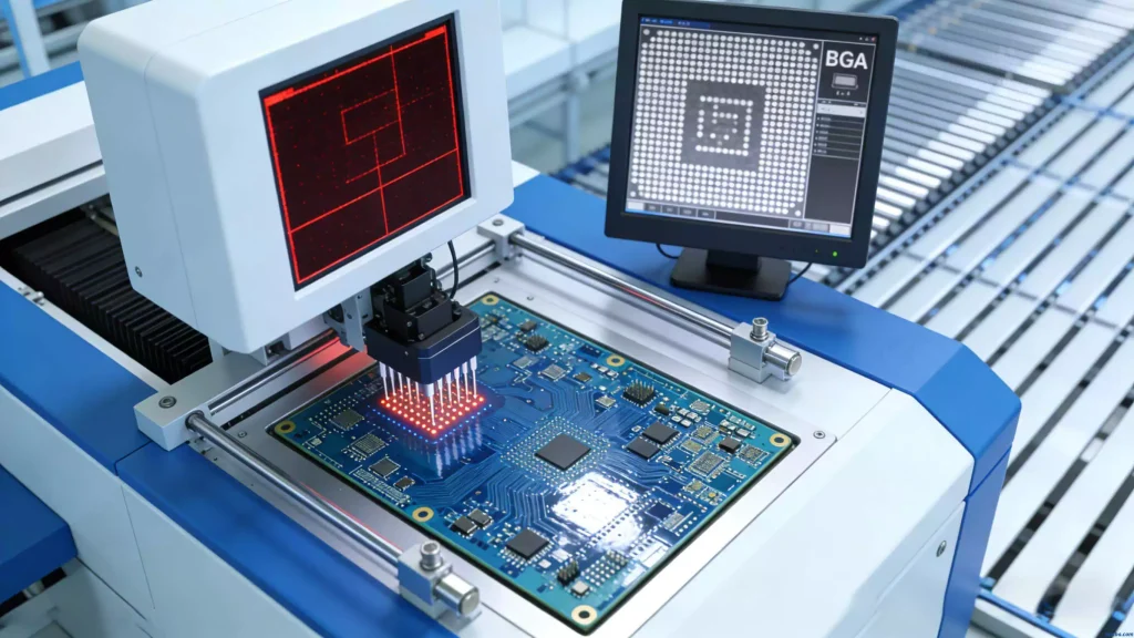
Use AOI and probe testing. They catch issues pre-assembly. For critical communication devices, add X-ray on BGAs. Check plating and cleanliness too.
Future Directions: 6G and Beyond in Circuit Board Design for Communication Devices
6G will use terahertz bands and AI reconfiguration. PCBs may shift to glass substrates for low loss. 3D integration and photonics will grow in future communication devices.
Flexible PCBs suit foldable cells or satellites. Additive methods print conformal antennas. These simplify builds for next-generation communication devices.See how similar technologies apply in [medical equipment PCBs]
We invest in these areas. This keeps clients ahead in wireless communication technology for communication devices.
In summary, the circuit board shapes performance and reliability in every communication device. Master materials, layout, and manufacturing. This turns ambitious wireless ideas into top products for communication devices.


