High-Density Wiring & Superior Electrical Performance for PCB
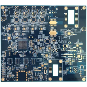
Overview of HDI PCB
HDI circuit boards outperform ordinary multi-layer PCBs.
Their core advantages lie in “precision” and “efficiency”.
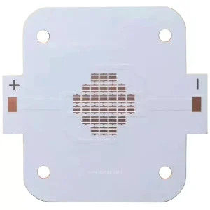
They are high-end printed circuit boards.
They use advanced precision processes, including high-density wiring, small hole diameters, and blind vias.
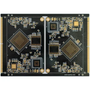
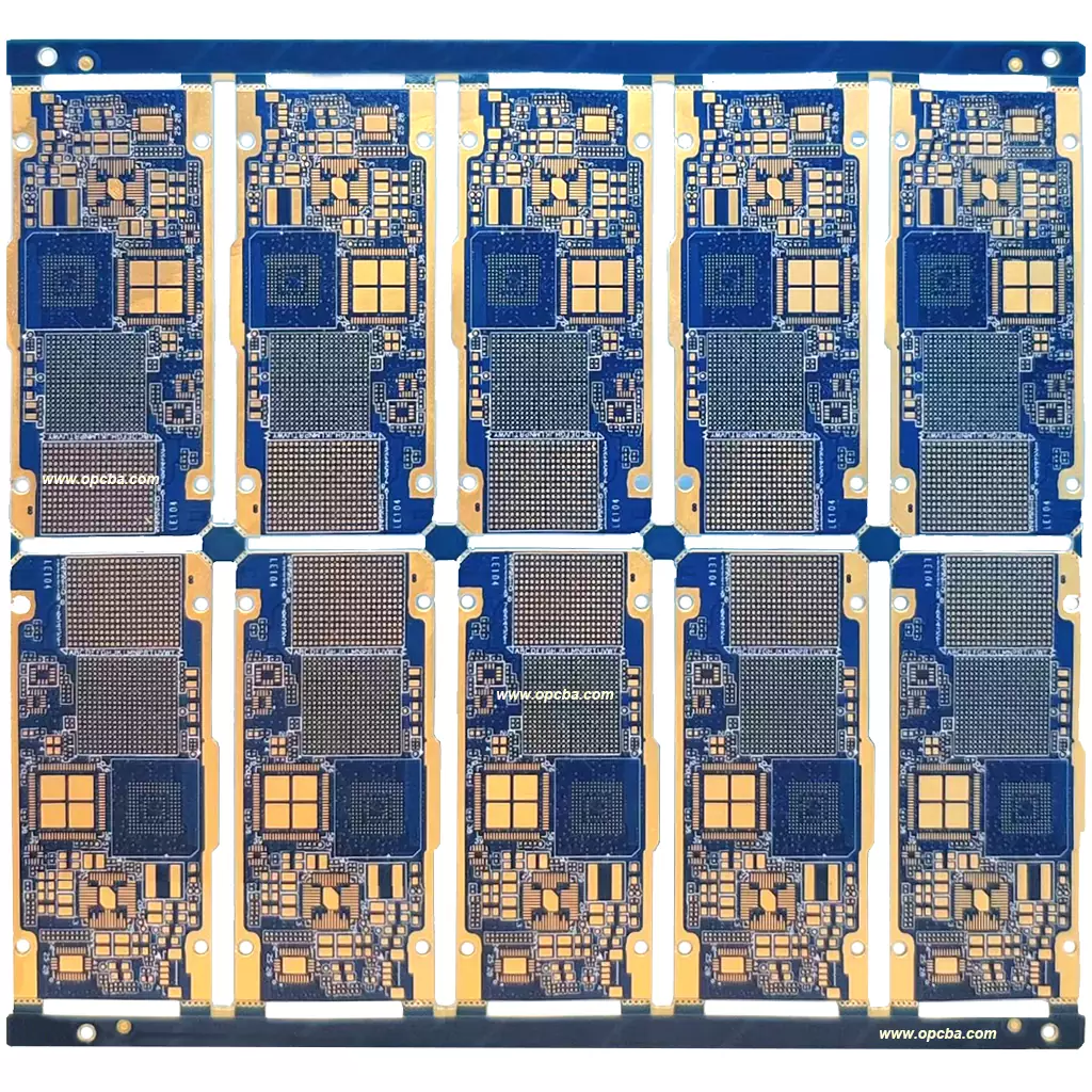
Structural Composition
HDI circuit boards are classified by their number of blind-buried holes.
The categories are:
-
Low-order: 1–2 orders of blind-buried holes
-
Medium-order: 2–3 orders of blind-buried holes
-
High-order: 3–4 orders and above
Key Design Considerations
The core principle of HDI circuit layout is “fine wiring + interference isolation”.
Outer Layers
Line width and spacing must match component pin density.
-
Conventional specs: ≤3 mil
-
High-grade specs: 1–2 mil
This avoids line intersections and excessive length.
Inner Layers
Strictly separate power, ground, and signal lines.
Use a “power-ground” paired layout to reduce crosstalk.
High-Frequency Signals
Require impedance matching (e.g., 50Ω, 100Ω).
This reduces signal attenuation.
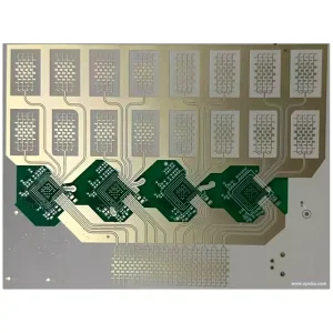
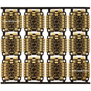
Multi-Field Applications
HDI circuit boards act as the “core neural network” of high-end electronic devices.
They are widely used across many industries:
-
Consumer electronics, communications, automotive electronics
-
Medical devices, artificial intelligence, aerospace and military
They directly impact the accuracy and stability of terminal devices.
They are core components of high-end electronic manufacturing.
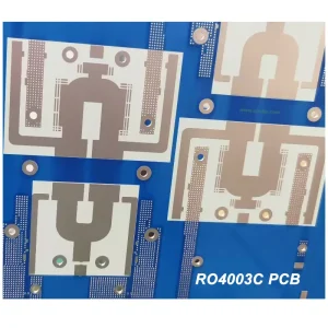
Material Selection & Cost Reference
HDI circuit boards are primarily made of high-performance FR-4 glass fiber epoxy resin.
For high-end applications, they use additional specialized materials:
-
High-frequency, high-speed options: Rogers, PTFE
-
High-Tg and halogen-free materials
They also use 2–5μm ultra-thin copper foil.
This ensures excellent heat resistance, insulation, and signal transmission.