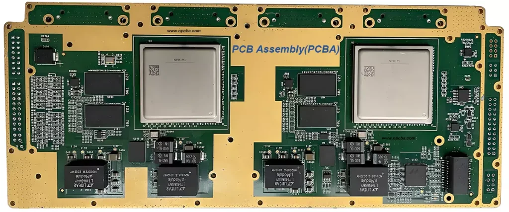
PCBA refers to the process of transforming a bare PCB into a functional finished product through SMT mounting, DIP insertion, and rigorous testing. This assembly is the backbone of nearly all electronic devices, from consumer gadgets to industrial equipment, as it integrates electronic components to deliver the intended functionality.
The production process of PCBA board is very complex. It includes PCB fabrication, component sourcing, SMT placement, DIP insertion, and final validation. This complexity makes board assembly testing an indispensable step for quality and reliability.
What is PCBA?
PCBA = Printed Circuit Board Assembly, PCB’A is commonly used in European and American standards. The PCB board is precisely assembled with electronic components such as chips, resistors, capacitors, etc. through SMT and DIP soldering processes to form the PCBA, which realizes various functions of electronic products.
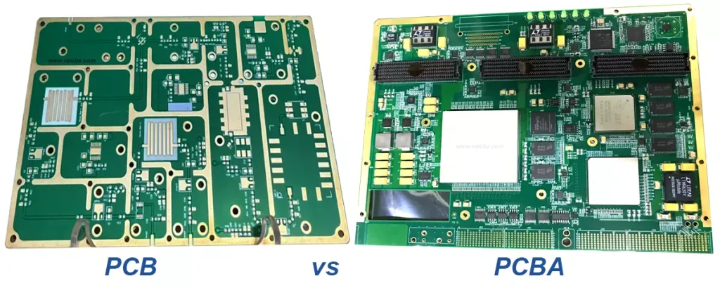
The difference between PCB vs PCBA
PCB is just a bare circuit board without any components installed, only wires and solder joints. PCB only realizes circuit graphic wiring, and PCB manufacturing includes basic processes such as etching and drilling.
PCBA is a functional circuit system that completes the assembly of components. PCBA integrates components to achieve complete circuit functions (such as signal processing, power conversion, etc.), and PCBA requires SMT mounting, DIP plug-in and other assembly technologies.
The PCBA board already has the electrical connections and functions required by the design, and is the core hardware part of the entire electronic product. After receiving the PCBA, electronic product manufacturers install it into the casing and connect other components (resistors, capacitors, integrated circuits, etc.) to form the final electronic product.
PCBA is an essential core component in electronic devices, which carries the electrical connections between electronic components and is the key to achieving device functionality.
The characteristics of PCBA are mainly reflected in its high precision, high reliability, and high integration. Modern electronic devices have increasingly high performance requirements for circuit boards, and PCBA manufacturers need to adopt advanced production processes and equipment to ensure product quality.
Common PCBA production processes include surface mount technology (SMT), wave soldering, reflow soldering, etc. These processes can achieve high-precision installation and reliable soldering of components.
Why choose PCBA one-stop service?
Customers used to purchase PCB circuit boards and components separately, but now more and more customers hope Opcba can provide one-stop PCBA services for PCB + electronic components.
Opcba conducts audits on component suppliers to confirm whether they are genuine components. The sales channels for electronic components are networked, and prices tend to be transparent. Customers may end up purchasing components at the same price as Opcba, which is equivalent to spending the same amount of money to do more things.
The one-stop PCBA service includes the entire budget, controllable prices, no other costs, reduces uncertainty, and lowers costs to cope with uncertainty.
Customers may not be familiar with the current price trends of PCB circuit boards and components, as well as new SMT technologies. But as a PCBA manufacturer, Opcba has to handle these backend processes every day. Handing over professional tasks to a more professional team, Opcba engineers are very clear about what kind of PCB board and solder paste to use in what industry.
The most important thing is that PCBA manufacturers have many customers and a high demand for parts procurement. Correspondingly, customers can obtain more terminal channels, thereby obtaining more products, so the price will definitely be lower and the quality will definitely be guaranteed.
Opcba specializes in high-end SMT assembly and PCBA testing, equipped fully automated high-speed SMT lines, SPI solder paste thickness detectors. AOI optical inspection systems, X-ray machines, and reflow ovens. The facility supports the placement of precision components, including 01005 chips, 0.3mm Pitch BGA, and QFN packages.
How to obtain an accurate PCBA quotation?
When outsourcing the manufacturing of your printed circuit board (PCB), electronic box, or cable assembly to an electronic contract manufacturer, you hope to obtain a fast and accurate quotation in advance. Putting accuracy first from the beginning is in line with the best interests of EMS manufacturers.
Here are some tips on what measures you can take to ensure accurate PCBA quote and reduce the chaos of frequently delayed projects:
To provide useful quotation information for your electronic contract manufacturer, please pay attention to the following four areas of detail for faster and more accurate electronic subcontracting manufacturing quotations.
- PCB files and PCB production requirements
- BOM List
- Component coordinate file
- Inspection and testing requirements
- Other key information for production and manufacturing
- In addition, the shipping address and manufacturing quantity also affect the PCBA quotation
Opcba receives the documents and conducts preliminary DFM analysis on the components and manufacturing processes, followed by progress PCB quotation and PCBA quotation.
If you are unsure if certain information needs to be included, please contact your PCBA manufacturer. Receiving accurate quotes from the beginning enables you to compare PCBA quotes more effectively, ultimately saving you time, money, and pressure. High quality PCBA can quickly and successfully launch your product and win market success.


