Cameras have evolved beyond mere peripheral components of electronic devices to become indispensable parts of core systems in smartphones, autonomous vehicles, AI terminals, and more. At the heart of this visual revolution lies the camera module PCB—a compact yet powerful circuit board designed to efficiently connect image sensors with digital systems. Whether you’re an electronics designer, engineer, or procurement professional, understanding camera module PCBs is crucial for driving product innovation.
What is a Camera Module PCB?
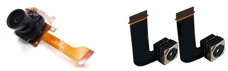
A camera module PCB is a specialized circuit board integrating the following core components:
Image sensor (CMOS or CCD)
Lens assembly
Image signal processor (ISP)
Power supply regulation circuitry
Transmission interfaces (e.g., MIPI CSI, USB, LVDS, or DVP)
It serves both electrical connectivity and structural support functions, acting as the bridge between the camera module and the host device.
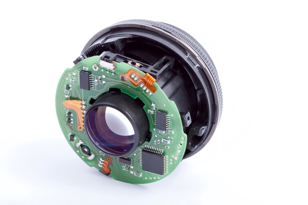
Key Components of a Camera Module PCB:
Image sensor (CMOS/CCD): Converts light into electronic signals
Lens system: Focuses light onto the sensor surface (fixed focus or autofocus)
ISP Chip: Optimizes image quality by adjusting exposure, white balance, color, etc.
Regulator Circuit: Provides a stable power supply
High-Speed Connector or Flexible Flat Cable (FFC/FPC): Connects to the main control board for image data transmission
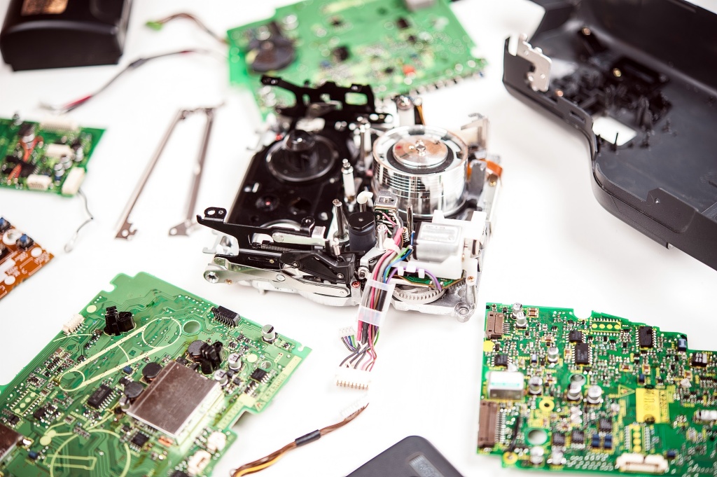
Key Manufacturing Processes for Camera PCBs:
1. Design and Prototyping
Camera PCB production begins with meticulous design and prototyping. Engineers utilize advanced computer-aided design (CAD) software to create intricate layouts that optimize space and performance. The design phase requires careful consideration of factors like signal integrity, power distribution, and thermal management. Rapid prototyping techniques—including 3D printing and CNC machining—enable swift design iteration and testing to ensure compliance with specific requirements before full-scale production.
2. Material Selection
Material choice is critical to camera PCB performance. High-frequency materials like FR-4, Rogers, and polyimide are typically used to support signal integrity and minimise interference. Substrates must withstand environmental challenges, particularly in outdoor applications where humidity, temperature fluctuations, and UV exposure can severely impact performance. Selecting appropriate solder masks and surface finishes is also vital for enhancing durability and ensuring reliable connections.
3. Manufacturing Techniques
We employ state-of-the-art manufacturing techniques to produce camera PCBs. Precision drilling and laser cutting ensure each PCB meets exact specifications. Etching technology removes excess copper to create necessary circuit paths while minimising waste. Multilayer designs integrate complex circuits, enabling advanced functionality within compact spaces. Automated processes enhance accuracy and reduce manufacturing time, shortening customer turnaround while maintaining quality.
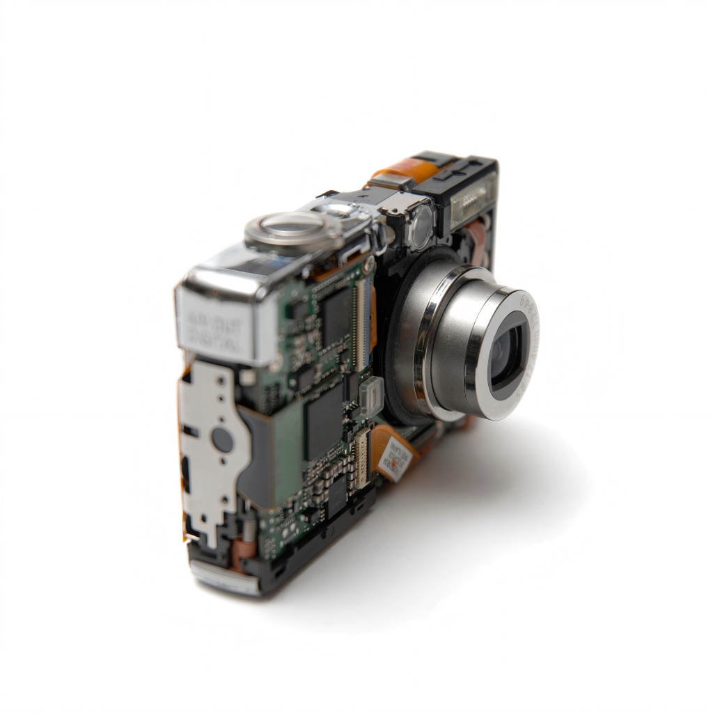
4. Assembly Process
Once components are manufactured, assembly is critical. Advanced soldering techniques, including Surface Mount Technology (SMT) and through-hole soldering, ensure robust connections. The assembly process typically involves placing numerous small components, demanding precision and efficiency. Automated pick-and-place machines guarantee consistent component placement, minimising human error risks and boosting production speed. Additionally, reflow ovens ensure solder is fully melted and cooled, forming strong, reliable joints.
5. Testing and Quality Assurance
Rigorous testing protocols are essential for ensuring the reliability of camera PCBs. This includes electrical testing to verify each PCB for short circuits, open circuits, and proper functionality of all components. Thermal cycling tests simulate environmental stresses, confirming the PCB’s ability to withstand extreme temperature variations. Environmental stress testing evaluates PCB performance under conditions such as humidity and UV exposure. Quality assurance measures validate each PCB’s compliance with industry standards, providing confidence to both manufacturers and end-users. Certifications like ISO 9001 and IPC-A-610 ensure continuous improvement in manufacturing processes and adherence to stringent quality benchmarks.
Key Considerations for Camera Module PCB Design:
1. When using connectors: For MIPI differential signals passing through connectors, adjacent differential pairs must be isolated using GND pins. If plating through holes is impractical, maintain a minimum spacing of 15 mil between differential pairs. Apply a continuous ground plane, with ground vias placed every 200 mil.
2. If the camera connector features reserved test points, position them near the connector and minimize stub lengths on routing traces.
3. Decoupling capacitors for the AVDD/DOVDD/DVDD power pins of the connector should be placed as close as possible to the camera connector.
4. During camera layout, maintain distance from high-power radiating components such as GSM antennas.
5. For CIF/MIPI signals connected via board-to-board connectors, all signals should be series-terminated with resistors (2.2 ohm to 10 ohm, determined by SI test requirements) and equipped with TVS devices.
6. Differential traces crossing layers require adjacent return ground vias. Where space permits, implement strict ground plane coverage for signals.
PCB Design Considerations for MIPI CSI RX:
1. Decoupling capacitors for all camera power supplies must be retained and placed near the connector.
2. The camera’s Reset signal should be controlled via GPIO. The 100nF Reset capacitor must remain near the connector to enhance ESD protection.
3. The camera’s CLK clock line should be ground-tracked. Add GND vias every 300 mil along the ground track. If space does not permit, maintain a minimum 3W spacing between this track and any adjacent tracks.
Key Application Areas in 2025:
Consumer Electronics: Smartphones, tablets, laptops, smart glasses
Automotive Systems: Autonomous driving, parking assistance, panoramic imaging systems
Medical Devices: Endoscopes, portable imaging equipment
Industrial Applications: Robot vision, barcode scanning, intelligent inspection
Security Surveillance: Night vision cameras, AI facial recognition systems
Summary
In summary, camera module PCBs—as modular devices integrating key components like main control chips, lenses, and sensors—play a vital role in electronic equipment. Their complex structure and rich functionality meet diverse application demands across various fields. With ongoing technological advancements, the performance and application domains of camera module PCBs will continue to expand, delivering more convenient and high-quality imaging and surveillance experiences.


