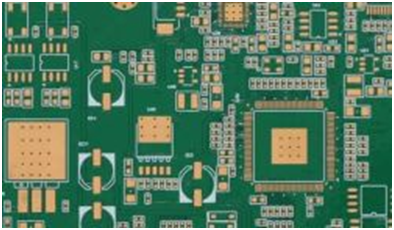
In the electronics industry, exposed copper PCBs are a crucial foundational material.
Exposed copper PCBs consist of copper foil, an insulating substrate, and an adhesive. Copper foil provides excellent electrical conductivity, ensuring fast, low-loss transmission of electronic signals.
With the advancement of electronic technology, the requirements for copper foil purity and thickness uniformity are becoming increasingly stringent. The latest manufacturing processes can produce copper foil with nanometer-level uniform thickness, ensuring more precise electronic circuits.
Exposed copper PCBs, with their simplified process, manageable costs, and flexible adaptability, have become a “secret weapon” for accelerating prototype turnarounds.
Many engineers habitually choose tin-plated or gold-plated pads for lab prototypes, unaware that using exposed copper pads can shorten prototype cycles by 40% and reduce trial-and-error costs.
1. Eliminating Plating Steps Significantly Shortens PCB Manufacturing Cycle Time
Eliminating Plating Steps Significantly Shortens PCB Manufacturing Cycle Time
Tin-plated pads
It involves three extra steps: pre-tinning, tin plating, and cooling. Each step typically takes 4–6 hours.
Gold-plated pads
They have an even more complex flow: nickel immersion, gold plating, and cleaning, with a total process time of 8–10 hours.Plating lines also create additional waiting time, especially for small-batch PCB fabricators often used by labs, who usually operate only one or two plating tanks.
In contrast, bare copper PCBs require only etching and cleaning after the circuit pattern is formed. The entire plating stage is completely eliminated.
In a real lab test using the same 2-layer PCB design with 50 pads:
Bare copper PCB prototype: 3 days
Tin-plated PCB prototype: 5 days
Gold-plated PCB prototype: 6 days
Bare copper PCBs are 2–3 days faster than conventional plated PCBs, perfectly matching the “rapid verification” demands of R&D teams.
For R&D labs and engineering teams that value speed, flexibility, and quick validation, bare copper PCBs are the most efficient choice for rapid prototyping.
2. Controllable Costs: Reduced “Trial and Error Costs,” Effortless Multiple Iterations
Laboratory prototyping often involves multiple rounds of trial and error—it may take two or three prototypes to resolve design issues. Exposed copper PCBs offer lower costs and allow for bolder, faster iterations.
Prototyping unit price is 30%-50% lower, making multiple iterations more cost-effective
Laboratory prototyping typically requires a small number of PCBs (5-20 pieces), and unit price significantly impacts total cost. For example, consider a commonly used two-layer board (100mm x 80mm, 50 pads) in a laboratory:
If R&D requires three rounds of prototyping, bare copper PCBs save 1,200 yuan compared to tin-plated PCBs and 3,000 yuan compared to gold-plated PCBs. For labs with limited budgets (such as university labs and startup R&D departments), the cost advantage of bare copper PCBs can support more rounds of design optimization, accelerating the search for the optimal solution.
3. Flexible Adaptability: Meeting Diverse Laboratory Prototyping Needs
Laboratory prototyping requires a wide range of PCB types, including low-frequency signal boards, high-current power boards, and temporary test fixtures.
Exposed copper PCBs can flexibly adapt to these needs, eliminating the extra waiting time caused by mismatched plating.
Rapid verification of high-current scenarios without the need for custom plating
Laboratory development of power circuits (such as DC-DC converters and motor driver boards) often requires verifying high-current (2-5A) conduction capabilities.
The high conductivity of bare copper PCBs (58MS/m) perfectly meets this requirement, eliminating the concern associated with tin-plated PCBs, which may melt at high temperatures and affect current conduction.
Quickly create temporary test fixtures, ensuring they are disposable after use.
Laboratories often need to create temporary test fixtures (such as PCB continuity test fixtures and sensor calibration fixtures). These fixtures have a short lifespan (1-2 months) and
are used only for internal testing. Long-term corrosion resistance is not a concern, so bare copper PCBs are the best choice.
For R&D personnel, choosing bare copper PCBs is not a “second best option” but a “precise match to needs” – the core goal of product prototype development is to “quickly verify the design” rather than pursuing mass production-level coating protection, and Exposed copper PCBs just perfectly fit this goal.


