What is PCB surface finish?
PCB surface finish refers to the metallization of the exposed copper areas on a printed circuit board that are intended for soldering, as well as the connections between these areas and the components. A PCB has a copper substrate surface; without a protective coating, this surface is highly susceptible to oxidation, making surface finish essential.
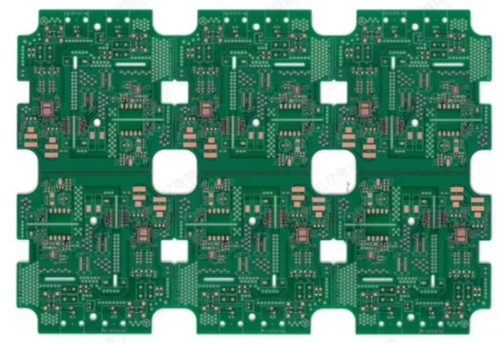
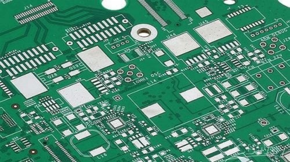
PCB surface finish is the most critical step in the PCB manufacturing and assembly process, serving two primary functions: protecting the exposed copper circuits and providing a solderable surface for attaching components to the PCB during soldering. As shown in the figure below, the surface finish is located on the outermost layer of the PCB, above the copper layer, acting as a “coating” for the copper.
Types of PCB Surface Finish
- Hot Air Solder Leveling (HASL)
- Immersion Tin (ImSn)
- Electroless Nickel Immersion Gold (ENIG)
- Organic Solderable Paste (OSP)
- Immersion Silver (ImAg)
- Electroless Nickel, Electroless Palladium, Immersion Gold (ENEPIG)
- Hard Gold (Electrolytic Hard Gold)
6 Major PCB Surface Finish Processes: Characteristics, Advantages and Applications
Currently, there are six mainstream PCB surface finish processes in the industry, each with its own advantages and disadvantages, suited to different product requirements and cost budgets. A detailed comparison is as follows:
OSP (Organic Solderability Protective Layer)
- Principle: We form an ultra-thin organic protective film—typically made of imidazole or benzotriazole compounds—on the copper foil surface via chemical deposition. This film measures just 0.1–0.3 μm thick and does not alter circuit impedance. During soldering, the solder dissolves this protective layer, exposing the active copper surface.
- Advantages: Low cost (only an additional 0.1–0.3 RMB per board), simple process, and high production efficiency; lead-free and environmentally friendly, compliant with RoHS standards; does not increase PCB thickness, suitable for high-density, fine-pitch components (such as 0402 packages and QFP chips); minimal impact on impedance, suitable for high-frequency PCBs.
- Limitations: The protective film is prone to moisture absorption and requires strict storage conditions (dry environment required, shelf life of 3–6 months); poor temperature resistance, with a maximum of 2 reflow soldering cycles (failure likely beyond this limit); not suitable for long-term outdoor or humid environments.
- Applications: Consumer electronics (mobile phones, power banks, routers), small appliance control boards, and other products with high volume, cost-sensitive requirements, and favorable storage conditions; high-frequency PCBs (e.g., 5G router motherboards).
Hot Air Solder Leveling (HASL)
- Principle: We immerse the PCB in molten solder—traditionally a Sn-Pb alloy, now mostly a lead-free Sn-Ag-Cu alloy—and then use a hot air knife to level the solder layer. This process forms a uniform tin layer measuring 2–20 μm thick.
- Advantages: Lower cost (an increase of 0.5–1 RMB per board), mature process, and high stability; good solder wettability and strong soldering reliability; good temperature resistance, with up to 3–5 reflow cycles; lenient storage conditions (shelf life of over 1 year), suitable for bulk storage and transportation.
- Limitations: The surface flatness of the tin layer is relatively poor (minor irregularities remain after leveling with the hot air knife), making it unsuitable for ultra-fine-pitch components (such as 0201 packages and BGA chips); the melting point of lead-free spray tin is high (217°C), posing a risk to components with poor heat resistance; uneven tin layer thickness may affect impedance.
- Applications: Industrial equipment (power modules, controllers), automotive electronics (non-critical areas), security equipment, and other products requiring high soldering reliability and cost-effectiveness; PCBs with wide component spacing (≥0.5 mm).
Immersion Gold (ENIG)
- Principle: Through chemical deposition, a layer of nickel (2–5 μm thick) is first plated onto the copper foil surface, followed by a layer of gold (0.1–0.3 μm thick). The nickel layer acts as a barrier to prevent diffusion between the gold and copper, while the gold layer provides excellent soldering and contact performance.
- Advantages: Extremely high surface flatness, suitable for ultra-fine pitch and precision components (such as BGA, CSP chips, and 0201 packages); high corrosion resistance, suitable for harsh environments such as outdoor, humid, or acidic/alkaline conditions; long shelf life (1–2 years) and high soldering reliability; good electrical conductivity, suitable for connector contact points (such as SIM card slots and USB ports).
- Limitations: Higher cost (an additional 2–3 RMB per piece), complex manufacturing process, and long production cycle; risk of “black pad” (soldering defects caused by nickel layer oxidation), requiring strict process control; the gold layer is relatively thin, making it unsuitable for multiple reflow soldering cycles (≤3 times).
- Applications: High-end consumer electronics (flagship smartphones, smartwatches), high-frequency communication equipment (5G base stations, RF modules), medical devices, automotive electronics (ECU, BMS), and other products requiring high reliability and precision; connector interface areas.
Immersion Silver
- Principle: A layer of pure silver (0.5–2 μm thick) is formed on the copper foil surface through chemical deposition. The silver layer exhibits excellent electrical conductivity and forms an alloy with solder during the soldering process.
- Advantages: Surface flatness is comparable to immersion gold, making it suitable for fine-pitch components; excellent electrical conductivity with minimal high-frequency signal loss; lower cost than immersion gold (an increase of 1.5–2.5 RMB per board); The process is less complex than gold plating, resulting in higher production efficiency.
- Limitations: The silver layer is prone to oxidation and discoloration (especially in humid environments); it has a relatively short shelf life (6–12 months); its corrosion resistance is inferior to gold plating, making it unsuitable for long-term outdoor use; there is a risk of “silver migration” (silver ions may migrate in humid environments, causing short circuits).
- Applications: Mid-to-high-end consumer electronics (tablets, mid-range smartphones), high-frequency PCBs (e.g., router RF boards), and other products requiring precision and conductivity but with a budget lower than that of immersion gold; devices intended for short-term storage or indoor use.
Electroless Palladium Immersion Gold (EPIG)
- Principle: A palladium layer (0.1–0.3 μm thick) and a gold layer (0.05–0.1 μm thick) are sequentially deposited onto the copper foil surface. The palladium layer replaces the nickel layer found in electroless gold plating, providing superior barrier and anti-oxidation properties.
- Advantages: Completely eliminates the “black disk risk” associated with immersion gold, resulting in higher soldering reliability; superior corrosion resistance and wear resistance compared to immersion gold; high surface flatness, suitable for ultra-precision components; excellent electrical conductivity, suitable for high-frequency and high-speed signal lines.
- Limitations: Extremely high cost (an increase of 5–8 RMB per piece) and high process complexity; only a few manufacturers have the production capacity, leading to supply chain constraints.
- Applications: High-end products with stringent reliability and performance requirements, such as aerospace electronics, high-end medical equipment, and ultra-high-frequency communication equipment (e.g., satellite communication modules).
Electroplated Gold
- Principle: Deposits a gold layer on the surface of copper foil via electrolysis, with precisely controllable thickness (0.5–5 μm). No intermediate nickel or palladium layers are required; the gold layer features high purity and excellent conductivity.
- Advantages: Thick gold layer with high wear resistance, suitable for connectors subject to frequent plugging and unplugging (e.g., test probe interfaces and high-frequency connectors); excellent conductivity with minimal signal loss; exceptional corrosion resistance, suitable for extreme environments.
- Limitations: It costs more since we bill based on gold layer thickness — adding 1–2 RMB per μm per board. The process is complex and results in a long production cycle. A thicker gold layer can negatively affect circuit impedance, so we do not recommend full‑board coverage. Instead, we typically apply selective plating only to specific areas.
- Applications: Products requiring extremely high wear resistance and conductivity, such as those in aerospace, electronics, and high-frequency testing equipment; localized connector interfaces (e.g., PCB test points, high-frequency connectors).
Conclusion:
In summary, the PCB surface finish type must be selected to fulfill various functional requirements. Each type of surface finish has its own advantages and disadvantages. There are engineering techniques available to address issues caused by the shortcomings of a particular surface finish. For example, to mitigate the low wettability of OSP, solutions include modifying the solderability plating or wave soldering alloy on the board or increasing top-side preheating. The key is to consider all possible factors to achieve optimal performance.


