Copper foil is the conductor in a PCB, and its thickness sets how much current a trace can carry, how well the board sheds heat, and what the finished board costs. Thickness is quoted by weight rather than by dimension: 1 oz means one ounce of copper per square foot, which becomes about 35 µm or 1.4 mil once the foil is laminated. The grades run from 0.5 oz for fine-line work up to 3 oz and heavier for power boards, and flexible circuits use a separate, thinner set.
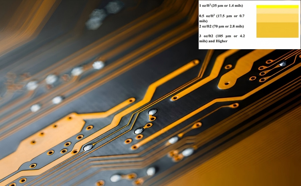
Standard Copper Thicknesses in PCB Design
- 1 oz/ft² (35 µm or 1.4 mil). The default for most boards on the market, and the grade that suits general-purpose circuits with moderate current and ordinary board sizes.
- 0.5 oz/ft² (17.5 µm or 0.7 mil). Used where space is tight or the load is light, and the usual choice for fine-pitch designs in small devices.
- 2 oz/ft² (70 µm or 2.8 mil). The step up for high-current work, where a trace has to carry more amperes without running hot.
- 3 oz/ft² (105 µm or 4.2 mil) and above. Heavy copper, reserved for power supply boards, automotive electronics, and anything that has to move a lot of current without overheating.
For most designs the choice lands on 1 oz/ft², moving to 2 oz/ft² where current demands it. That range balances electrical performance against what the fabricator can etch and laminate without a cost step.
Copper Thickness for Flexible Circuits
Flexible printed circuits use thinner foil, commonly 9 µm, 12 µm, and 18 µm. The lower weight is what makes the circuit bend without cracking the copper, which is why flex appears in wearables and inside phones where the cable has to fold into a hinge.
- 9 µm and 12 µm. Light enough for a wristband to sit flat on the arm while still carrying signal, and thin enough to survive repeated flexing in a tight radius.
- 18 µm. The step up where the circuit needs more mechanical strength or better conductivity, such as the display cable in a phone that bends every time the device opens.
Copper Thickness for Special Applications
Two ends of the range fall outside the standard grades.
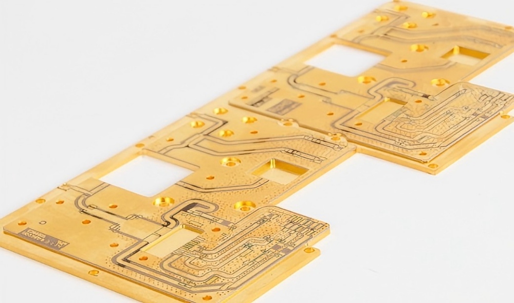
- Extra-thick foil. On an FR-4 base, heavy-copper processes take the foil to 2 oz (70 µm) and beyond, through 4 oz (140 µm) and 5 oz (175 µm). These boards are built for current transfer and heat spreading rather than for routing density: heavy copper boards turn up in power conversion, planar transformers, and high-power equipment.
- Ultra-thin foil. The other direction is driven by loss. Foil at 3.5 µm is in production and carrier-supported grades go below that, aimed at fine-line HDI, IC substrates, and the highest-speed channels, where a thinner conductor and a smoother surface both cut attenuation.
Three Factors That Decide the Thickness
Thicker is not automatically better. Three requirements decide it, and they do not always agree: the current sets a floor on the copper area, the thermal path wants more of it, and the signal path penalizes it.
Current-Carrying Capacity
Doubling the copper thickness roughly halves the resistance, so capacity rises faster than thickness does: 0.5 oz to 1 oz adds about 60% more current, and 1 oz to 2 oz adds roughly another 65%. The absolute numbers depend on the layer and on the temperature rise the design allows. Under IPC-2221, a 1 mm wide trace on an external layer at a 10 °C rise carries about 1.45 A at 0.5 oz, 2.4 A at 1 oz, and 3.9 A at 2 oz. The same trace on an inner layer carries roughly half that, because buried copper has no surface and no airflow to shed heat into. Working the sum the other way, from a required current back to a width, is what the trace width and spacing calculation covers.
Heat Dissipation
Copper conducts heat at about 401 W/(m·K); FR-4 sits at 0.3 to 0.5 W/(m·K). That gap means copper thickness, and the copper area left on the board, do most of the heat spreading. A low-power part such as a phone application processor runs on thin foil with convection from the board surface as the only path. An automotive MCU needs thicker foil to move heat into a sink. A traction inverter needs heavy copper plus thermal vias and a metal enclosure, because no amount of foil alone will carry that load away.
Signal Integrity
At high frequency the current crowds into the surface of the conductor, so the skin depth shrinks and the surface profile starts to matter as much as the bulk. Above 1 GHz, 1 oz or thinner is the usual choice, because thicker foil comes with a rougher treatment side, and roughness turns into attenuation. Below 100 MHz the thickness barely affects the signal, and 1 to 2 oz can be picked on current alone. Where a trace has to hold a target impedance, width and thickness have to be chosen together, which is what controlled impedance work covers.

Copper Foil Type and Thickness
Electrolytic and rolled copper are made differently and end up in different places. Electrolytic foil runs from 0.5 to 5 oz, has a rougher surface, costs less, and covers most current-carrying and heat-spreading work. Rolled foil runs from 0.3 to 2 oz, is smoother and more ductile, and suits high-frequency work and flexible circuits, where the grain structure has to survive bending.
Applications by Copper Thickness
What the grade is used for, in practice:
- 0.5 oz/ft². Low-power circuits, fine pitch, and space-constrained products: phones, wearables, and other compact devices that draw little current and need fine traces.
- 1 oz/ft². The general manufacturing grade, and the most common weight on the market. Consumer electronics, telecom equipment, and computers all run on it, because it balances capacity against manufacturability.
- 2 oz/ft². High-current circuits and power sections: power supplies, motor drivers, and automotive control units. Higher current, less heating, and a board that can take the load.
- 3 oz/ft². Heavy-duty power electronics, electric vehicles, industrial distribution, and renewable energy. The advantage is current and heat; the cost is a harder etch, more lamination cycles, and a higher price.
Summary
Copper thickness is one of the few design choices that changes current capacity, thermal behavior, signal loss, and unit cost at the same time, which is why it is usually settled early, with the stackup rather than after routing. The practical sequence is to size from current and allowed temperature rise, check the signal path against skin depth, then confirm the fabricator can hold the resulting line width and foil weight. HDI stacks and high-speed laminates keep pushing both ends of that range, so the grade is worth re-checking at each stackup revision instead of carrying over from the last board.