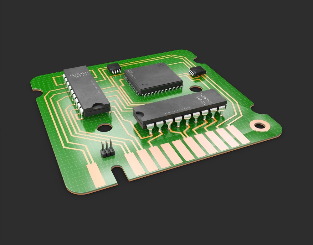
The manufacturing of a PCB (Printed Circuit Board) is a complex and precise process involving multiple steps, each critical to the performance and quality of the final product. From design, layout, printing, etching, drilling, copper plating, tin plating, cutting, testing, to final packaging, every step requires precise execution and strict quality control. The entire process demands advanced technical expertise and equipment support. Below is the detailed manufacturing process for PCBs:
Material Selection
PCB substrates typically consist of glass-fiber-reinforced epoxy (FR4), ceramic, or polyimide materials. Copper foil serves as the material for forming conductive paths. The choice of substrate and copper foil determines the circuit board’s mechanical strength, electrical conductivity, and thermal stability.
Substrate Selection: Choose an appropriate base material based on the PCB’s design requirements. Common substrates include FR-4 (epoxy glass cloth laminate), which offers excellent insulation, mechanical strength, and cost-effectiveness, making it suitable for most general electronics. For high-performance, high-frequency applications, specialized substrates like polytetrafluoroethylene (PTFE) may be chosen due to their low dielectric constant and low loss factor, facilitating high-frequency signal transmission.
Copper Foil Selection: As the conductive layer of the PCB, copper foil quality is critical. Common thicknesses include 1oz (approximately 35μm) and 2oz, selected based on the circuit’s current-carrying capacity. Properties like copper foil roughness and adhesion also require attention. Excessive roughness may compromise etching precision, while insufficient adhesion risks foil delamination during subsequent processing. Therefore, procure high-quality copper foil from reliable suppliers.
Other Auxiliary Materials: Including additional materials such as dry film, ink, chemical solutions (etching solutions, plating solutions, etc.), and drill bits. Dry film transfers circuit patterns, ink forms solder masks and character markings, chemicals play critical roles in etching and plating, while drill bits perform hole-making operations. Each material must be compatible with the appropriate specifications and brands based on process requirements to ensure smooth production.
Manufacturing Process
1. Internal Layer Fabrication:
Material Cutting: We cut large substrate sheets to PCB design dimensions to obtain the required board blanks. We must ensure dimensional accuracy and smooth edges, and we typically perform the cutting using CNC cutting machines.
Internal Layer Film Application: We apply dry film to the cut substrate via thermal pressing or vacuum bonding. The dry film adheres tightly to the surface to prepare for subsequent exposure.
Exposure: Transfer the designed inner layer circuit pattern onto the dry film using an exposure machine. This machine employs ultraviolet light to trigger a photochemical reaction in the dry film over the circuit pattern areas, rendering them insoluble in the subsequent developing solution and thereby fixing the circuit pattern.
Development: Immerse the exposed substrate in developer solution. Unexposed areas of the dry film dissolve, exposing the underlying copper foil and forming the preliminary internal circuit pattern.
Etching: We remove unwanted copper foil through chemical etching and leave only the circuit paths. This is a critical step in PCB manufacturing, because any error may cause circuit failure or short circuits. We must strictly control etching parameters—such as time, temperature, and solution concentration—to ensure circuit precision. We remove residual chemicals via rinsing after etching.
Stripping: We remove residual dry film on the inner layer traces using chemical solutions or mechanical methods and yield a clean inner layer board.
2. Laminating Process:
Browning Treatment: The inner layer board undergoes browning treatment to form a uniform oxide layer on the trace surfaces. This enhances adhesion to the prepreg and prepares the board for subsequent lamination.
Stack-up: Stack multiple inner-layer boards with prepreg and outer-layer substrates according to the predetermined laminate structure, ensuring precise layer alignment. The prepreg cures under high temperature and pressure, tightly bonding all layers together.
Lamination: We press the stacked board using a vacuum laminator. We precisely control temperature, pressure, and time parameters during lamination to prevent defects like bubbles or delamination. This process yields a multilayer board blank.
3. Outer Layer Circuit Fabrication:
Drilling: We use CNC drilling machines to create vias and mounting holes of various diameters based on the PCB design. We control drilling parameters such as speed and feed rate to ensure smooth hole walls and precise positioning, and to prevent problems such as broken drill bits or misaligned holes.
Copper Plating: We deposit a thin copper layer within the drilled holes to establish electrical connections between inner and outer layer circuits through vias. This process ensures uniform copper thickness and strong adhesion.
Full Board Plating: The entire PCB undergoes electroplating to thicken the copper layer, meeting requirements for electrical conductivity and mechanical strength. Post-plating cleaning removes residual plating solution from the board surface.
Outer Layer Film Application, Exposure, Development, Etching, Film Removal: This sequence mirrors inner layer circuit fabrication but targets the outer substrate. These processes form complete outer-layer circuits, establishing visible connections on the PCB surface.
4. Surface Treatment:
Solder Mask Application: We apply solder mask ink to the PCB surface. Through exposure and development, we expose the pad areas that require component soldering and cover the remaining areas with ink. This prevents short circuits during soldering and protects the circuits from external environmental corrosion.
Character Printing: We use screen printing or inkjet printing techniques to print component identifiers, model numbers, version codes, and other character information onto the PCB surface to facilitate subsequent assembly and maintenance.
Surface Finish Selection: Appropriate surface finish processes are chosen based on product requirements, such as electroplated gold, hot-dip tin, or OSP (Organic Solderability Preservative). Electroless gold plating offers excellent solderability and surface flatness, suitable for products demanding high soldering quality like mobile phone motherboards. Hot dip tin plating provides a cost-effective solution for general electronics. OSP strikes a balance between environmental compliance and cost, protecting pads from oxidation for a specified period and facilitating subsequent component placement.
Inspection and Quality Control
Visual Inspection: Conduct manual visual checks or utilize automatic optical inspection (AOI) equipment to examine PCB appearance. Verify absence of circuit defects like open circuits, short circuits, lifted copper foil, or faulty pads. Confirm the integrity and clarity of the solder mask and character printing to ensure visual quality compliance.
Electrical Performance Testing: Utilize specialized testing equipment such as vector network analyzers, oscilloscopes, and multimeters to evaluate the PCB’s electrical performance. This includes measuring parameters like circuit continuity, impedance, capacitance, and inductance to verify compliance with design specifications. Particular attention is given to high-speed signal lines to ensure signal integrity, promptly identifying and resolving any electrical performance issues.
Reliability Testing: To ensure long-term stable operation in diverse environments, reliability tests are conducted. These include thermal shock testing to simulate rapid temperature transitions between high and low environments, evaluating thermal stability; humidity testing to expose PCBs to high-humidity conditions and detect moisture-induced short circuits or metal corrosion; and vibration testing to mimic transportation and usage vibrations, checking for solder joint or component loosening/detachment. Only through rigorous reliability testing can PCB quality be guaranteed to meet the stringent demands of electronic products.
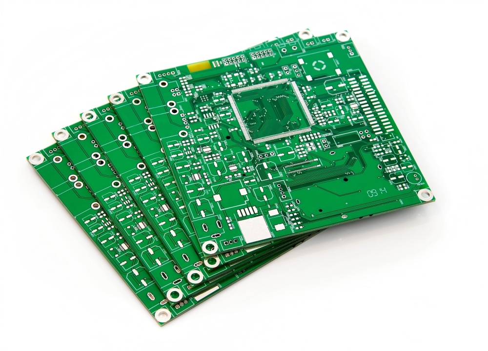
Finished Board Cutting and Packaging: After manufacturing, PCBs are cut to the final shape according to design specifications. They then undergo cleaning, inspection, and packaging before delivery to customers.
· Finished Board Cutting: CNC or laser equipment is to cut boards to the final dimensions.
· Packaging: Utilize anti-static or vacuum packaging to prevent damage during transit.
Conclusion
The PCB manufacturing process encompasses material selection, lamination, etching, drilling, plating, solder resist application, silk screen printing, surface finishing, and final testing and packaging. Each step is critical. Only through precise control of every process can high-quality PCBs be produced to meet the demands of complex electronic devices.


