Most signal-integrity failures on a high-frequency board are decided before a single trace is routed. They are decided in the stack-up. Layer sequence, dielectric choice, and reference-plane placement set the dielectric constant (Dk), the media thickness, and the return path. Those three set your impedance and insertion loss. Get the stack-up wrong and no amount of careful routing will rescue the board.
This guide covers how we build high-frequency multilayer boards: which materials to pick, where Rogers belongs versus FR-4, how impedance lives inside the laminate, and the warp trap that catches most hybrid builds. It is written for the engineer who releases the fabrication drawing and the buyer who specifies it.
1. Why the stack-up, not the trace, decides RF performance
Above 10 GHz, roughly 80% of the loss and impedance error traces back to the laminate stack, not the copper geometry on top of it. Three things the stack-up controls:
- Effective Dk of every transmission line. A 0.1 shift in Dk moves a 50 ohm line by several mils of width and changes phase length across the board.
- Media thickness between signal and reference plane, the biggest lever on characteristic impedance.
- Reference-plane continuity. Any slot, split, or missing plane under a line creates a local impedance bump and a radiation point.
A generic PCB stack-up treats all of this as make it symmetric. For RF, those details are the product. The rest of this article is about getting them right.

2. Know the materials: Dk, Df, and CTE
High-frequency laminates are judged on three numbers. Dielectric constant (Dk) sets speed and impedance. Dissipation factor (Df) sets loss. Z-axis CTE sets what happens when the board heats and cools.
| Material | Dk @10 GHz | Df @10 GHz | Z-CTE (ppm/°C) | Tg | Notes |
|---|---|---|---|---|---|
| Rogers RO4350B | 3.48 ±0.05 (design Dk 3.66) | 0.0037 | 32 | >280 °C | UL 94 V-0, most common RF workhorse |
| Rogers RO4003C | 3.38 ±0.05 (design Dk 3.55) | 0.0027 | 46 | >280 °C | No UL V-0, lowest-loss of the two |
| Isola 370HR (FR-4, high-Tg) | 4.17 | 0.0160 | 45 (below Tg) / 60-70 | 180 °C | Standard process, cheap, lossy |
| Astra MT77 / Shengyi mmWave77 | ~3.0 / 3.06 | 0.0017 / 0.0010 | low | n/a | 77 GHz radar / mmWave, FR-4 process compatible |
Two points engineers miss:
- Use the design Dk, not the process Dk. RO4350B’s printed Dk is 3.48, but field solvers should use the design Dk of 3.66. Impedance calculated on 3.48 comes back low on the test coupon.
- Copper roughness matters above 10 GHz. Standard HTE foil adds skin-effect loss. Specifying VLP (very-low-profile) foil on RF layers typically recovers 0.5 to 1.0 dB/inch at millimeter-wave frequencies.
If you want the full material data on our most-used Rogers grade, see Rogers 4350B performance characteristics.
3. Pure Rogers vs. hybrid (FR-4 + Rogers): cost and performance
Pure Rogers builds are the cleanest electrically and the most expensive. Rogers laminate runs roughly $45 to $80 per square foot against $8 to $12 for FR-4. For a board that is mostly digital but carries two RF channels, paying Rogers across all layers wastes money.
The standard answer is a hybrid stack-up: put Rogers only where the RF signal lives, and fill the rest with FR-4. This typically cuts Rogers consumption by 40 to 70% and saves $5 to $15 per prototype board.
A typical 6-layer hybrid:
- L1 : RO4350B thin core (RF microstrip)
- L2 : ground
- L3 : FR-4 (power / digital)
- L4 : ground
- L5 : FR-4 (digital)
- L6 : RO4350B thin core (RF)
The RF layers sit on Rogers; everything else rides FR-4. Done symmetrically, this is reliable and far cheaper than an all-Rogers board.
4. Impedance control lives inside the stack-up
Impedance is not a routing property. It is a stack-up property. The line width only expresses the impedance the laminate already allows. Representative numbers on RO4350B 10 mil core, 1 oz copper:
- 50 ohm microstrip: ~22 mil line width, ±5%
- 50 ohm GCPW (coplanar with ground): ~14 mil line / 8 mil coplanar gap
- 100 ohm differential microstrip: ~8 mil line / 6 mil space
Tolerances you can expect:
- Rogers single-ended: ±5% preferred / ±7% standard
- FR-4 single-ended: ±10%
- Differential: ±5% (Rogers) / ±10% (FR-4)
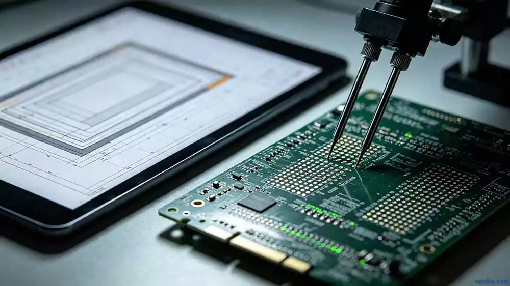
Two rules we repeat to every designer: media-thickness variation moves impedance directly, so tolerance starts with laminate thickness control. Always ask the fabricator for impedance simulation against their actual process parameters, not a textbook formula. For a deeper look at how shops actually hit the number, see our impedance control methods guide.
5. Warp control: where hybrid builds fail
Warpage is the main reason a hybrid panel rejects at SMT. Asymmetric copper and mismatched CTE between Rogers and FR-4 pull the board into a bow. A bad hybrid can show 2 to 3 mm per 100 mm of bow, well past the IPC-6012 Class 2 limit of 0.75%.
Three rules keep it flat:
- Mirror symmetry about the board centerline. Every layer and its copper weight should have a mirror on the opposite side of the mid-plane.
- Place Rogers layers in symmetric pairs. If L1 is Rogers, L6 should be too.
- Keep RF layers adjacent to a solid ground plane. Any split or slot under an RF line causes a local impedance step and a radiation site, not just a warp issue.
Acceptance targets: ≤0.75% for general SMT, ≤0.5% for BGA and fine-pitch assemblies.
One assembly note follows from this: fine-pitch RF devices demand a flat, solderable surface, and Hot-Air Solder Leveling (HASL) is not flat enough below ~0.64 mm pitch. For those designs, ENIG is the safer surface finish. The trade-offs are covered in our surface finish comparison.

6. Process capability: don’t just draw the electrical view
The stack-up drawing is only half the job. The other half is whether the shop can build it.
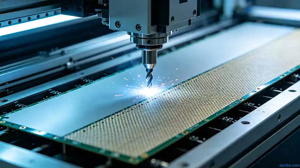
- Drilling: RO4350B drills on standard carbide tooling at ~±50 µm. PTFE-based grades (RO3000 family) need plasma desmear or activation, or the hole wall will not bond.
- Lamination temperature: RO4000 series cures at ≥190 °C, above the ~170 °C typical of FR-4. In a hybrid, the lamination profile must follow the Rogers curve, not the FR-4 one.
- Bonding ply: use RO4450F prepreg (Dk 3.52) in the RF signal path. Use plain FR-4 prepreg (2116 / 7628) only in structural, non-RF layers. That choice alone saves 40 to 60% on bonding cost.
7. Pre-fab checklist
Run this before releasing the gerber and fab notes:
- Stack-up is mirror-symmetric about the centerline.
- Every RF layer has a continuous, un-split reference plane.
- Media thickness uses standard catalog values (10 / 20 / 30 / 60 mil), not round numbers.
- Impedance tolerance is written into the FAB Notes, with target value and test-coupon requirement.
- Copper foil grade is specified per layer (VLP on RF layers above 10 GHz).
- Warp acceptance is stated (≤0.75% SMT, ≤0.5% BGA/fine-pitch).
- RO4450F is called out only in RF signal-path layers; FR-4 PP elsewhere.
- Lamination profile references the Rogers cure temperature, not FR-4.
- Surface finish is specified per assembly need (ENIG for fine-pitch RF).
- Design Dk (not process Dk) is used in the impedance model.
8. How to align with your PCBA factory
The cleanest stack-up still fails if the spec is vague. Write these five items into every RF fab package:
- Target impedance and tolerance (for example, 50 ohm ±7% single-ended, 100 ohm ±10% differential).
- Material by layer, exact grade and thickness, not Rogers or equivalent.
- Symmetry and warp limit in the stack-up notes.
- Coupon requirement: request an impedance test coupon from the production panel, not just a calculation.
- Copper and finish specs: VLP foil on RF layers, ENIG where fine-pitch applies.
A capable shop returns an impedance model built on its own process parameters, a symmetry check on the proposed stack-up, and coupon data from a previous similar build. If they cannot, that answer tells you what you need to know.
What we build to (typical capability, grounded in published Rogers fabrication data and standard IPC-6012 tolerances): controlled impedance at ±10% as the standard tolerance, with ±7% held on controlled-impedance orders and ±5% on Rogers RF builds where the design calls for it, each verified by TDR coupon on the production panel. We run Rogers cores down to 4 mil (0.10 mm) and build hybrid stacks from 4 to 20-plus layers.
9. FAQ
Can Rogers and FR-4 be mixed in one board?
Yes. It is standard practice for cost-sensitive RF designs. The constraint is symmetry and CTE management, covered in Section 5.
RO4350B or RO4003C?
Pick RO4350B when you need UL 94 V-0 or a general-purpose RF grade. Pick RO4003C when every 0.001 of Df matters, antennas, phased arrays, and low-noise front-ends.
Do I need Rogers above 10 GHz?
You need a material whose Dk tolerance holds the line. RO4350B holds ±0.05; standard FR-4 drifts ±0.3 to ±0.5, too loose for tight impedance at those frequencies.
How do I avoid hybrid warp?
Symmetry about the centerline plus Rogers in matched pairs. There is no shortcut.
10. Conclusion
A high-frequency board is won or lost at the stack-up. Choose the dielectric by Dk/Df and CTE, keep Rogers only where the RF signal runs, hold impedance with the fabricator’s real process model, and respect symmetry above all. Get those four right and the routing takes care of itself.
For the companion material deep-dive, start with Rogers 4350B performance characteristics, and for the general layup rules that this article specializes, see our PCB stack-up guide.