Your newest gadget just failed its thermal test, and you’re staring at a melted mess on the bench. The chip itself is fine, but its connection to the board? Not so much. This is the reality of hardware development: the partnership between the chip and the PCB can make or break a product. Get it right, and you have efficiency and reliability. Get it wrong, and you have a very expensive paperweight.
The Core Connection Between PCB and Integrated Circuits
Think of it this way: the PCB is the real estate, and the chip is the building. A microcontroller might be the central command center, while memory chips are the data warehouses. For advanced AI applications like ChatGPT, specialized high-performance chips (such as GPUs and NPUs) are required to handle the heavy computational load. The PCB’s job is to provide the land and the infrastructure—the roads (traces) and utilities (power planes)—so each building can do its job without interfering with its neighbors.
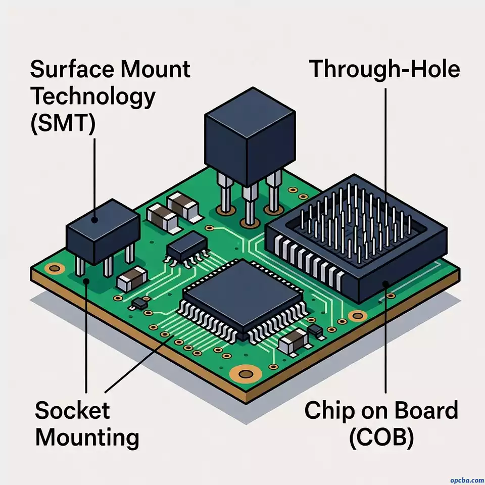
How does a chip actually attach to its board? It depends on the job it needs to do. For tiny passives and ICs in your phone, we use SMT—think of it as gluing components flat to the board to save space. For anything that needs to withstand physical stress, like a big connector, we might use Through-Hole, pushing the leads through the board and soldering them on the other side for a rock-solid hold. And for a CPU you might upgrade later, we don’t solder it at all; we give it a socket, like a docking station.
- Surface Mount Technology (SMT): Chips are soldered directly onto the PCB surface (the most common method for small, high-density designs).
- Through-Hole (DIP): Larger components have leads inserted through holes in the PCB and soldered on the opposite side.
- Socket Mounting: Chips like CPUs use sockets for easy replacement, rather than permanent soldering.
- Chip on Board (COB): Bare chips are directly bonded and encapsulated onto the PCB, eliminating traditional packaging.
The PCB’s job is twofold: it physically secures the chip and ensures stable electrical connections, so the chip can perform its function without interference or failure.
Chip Encapsulation: What It Is & Why It Matters
When discussing chips and PCBs, “chip packaging” is a critical term. Packaging protects the delicate bare chip from contamination and damage, while enabling electrical connections to the PCB. One specialized packaging method is Chip on Board (COB), where the bare chip is directly bonded to the PCB substrate, rather than being enclosed in a separate plastic or metal package. For many complex ICs, a dedicated IC substrate serves as the critical intermediate layer, bridging the chip’s delicate contacts to the larger PCB
How COB Assembly Works
COB packaging involves four key steps:
- Bonding: The bare chip is attached to the PCB using conductive or non-conductive adhesive.
- Electrical Connection: The chip is connected to the PCB via either wire bonding (thin gold/aluminum wires) or Flip Chip (FC) technology (direct solder bump connections).
- Encapsulation: The chip is covered with protective epoxy to shield it from dust, moisture, and physical damage.
- Testing: The assembled board is tested to ensure connections are stable and the chip functions correctly.
COB vs. SMT Encapsulation: Benefits & Tradeoffs
Traditional SMT packaging encloses chips in a separate package before soldering to the PCB, while COB skips this step. Each method has tradeoffs for performance, cost, and reliability:
Advantages of COB Technology
- Superior Thermal Management: SMT packaging creates multiple thermal resistance layers (package, solder, PCB), which trap heat. COB’s direct bonding simplifies the thermal path, reducing resistance and improving heat dissipation—critical for high-power chips.
- Cost Efficiency for High-Volume Simple Designs: For high-volume applications with relatively simple designs, COB can reduce production costs by removing the bill of materials for individual chip packages and streamlining the assembly process. However, this must be weighed against potential challenges in rework and testing, where SMT’s modularity offers a distinct advantage.
- Scalability for Multi-Chip Designs: COB is ideal for multi-chip or array packaging on a single substrate, making it perfect for high-density designs like LED arrays or sensor modules.
- Automation Compatibility: Most COB processes are easily automated, supporting large-scale production with consistent quality.
Disadvantages of COB Integration
- Substrate Limitations: COB places high demands on the substrate. While aluminum-based PCBs offer vastly superior heat spreading compared to standard FR-4, their performance is often limited by the thin, thermally resistive dielectric layer required for electrical insulation. Ceramic substrates, though pricier, bypass this issue with higher inherent thermal conductivity and a matched coefficient of thermal expansion (CTE), making them ideal for the most demanding high-power applications.
- Encapsulant Sensitivity: The performance of COB packaging depends heavily on the quality of the encapsulating epoxy. Poor-quality materials can lead to cracking, delamination, or thermal instability.
- Thermal Mismatch Risks: Chips, encapsulants, and substrates have different thermal expansion coefficients. Over time, temperature fluctuations can cause stress and failure if not carefully designed.
- Complex Heat Sinking: While COB improves heat dissipation in theory, designing effective heat sinks for COB assemblies can be complex and costly, especially for high-power applications.
Key Takeaways for PCB & Chip Integration
- COB is best for: High-power, high-density designs where heat dissipation and cost are critical (e.g., LED lighting, industrial sensors).
- SMT remains the workhorse of the electronics industry. It is best for: Designs requiring extreme miniaturization and high-speed automated assembly, such as the main logic boards in smartphones, tablets, and laptops. Its strength lies in the mature global supply chain for standardized components and the ability to densely populate both sides of a PCB.
- Always align packaging with your use case: The “best” method depends on your product’s performance, cost, and reliability requirements.
Choosing the right packaging isn’t just about the tech specs on a datasheet. It’s about balancing thermal performance, assembly yield, and long-term reliability against your budget. It’s a classic engineering trade-off. If you’re in the middle of navigating these decisions, talking to a manufacturing partner early can save you from costly prototype spins. At OPCBA, our engineers deal with these exact challenges daily—whether it’s simulating the thermal path for a COB design or optimizing a layout for high-speed SMT assembly. We’re happy to take a look at your project and offer a fresh perspective. For more resources or to discuss your project, visit opcba.com.


