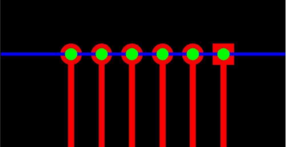
A castellated via PCB features rows of holes drilled along the PCB’s edge. We plate these holes with copper and trim the board edges, which effectively cuts the edge hole size in half and leaves visible copper inside the plated holes along the PCB edge.
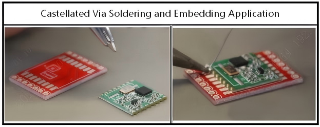
Designers generally equip module-type PCBs with castellated vias mainly to simplify soldering. As modular boards feature compact dimensions while supporting multiple functional needs, engineers typically place castellated vias along the PCB’s outermost edge. During contour routing, manufacturers route away half of each hole and retain only castellated vias on the PCB.
Advantages of Castellated Vias:
Incorporating castellated via into your PCB design offers significant advantages. Unlike standard connectors, plated through-hole PCBs can form stronger mechanical and electrical connections. Choosing surface-mount through-hole PCBs can optimize your manufacturing process and enhance the overall reliability of your product. It ensures a balance between performance and ease of assembly.
- Excellent Signal Integrity: The direct copper path along the edge of the through-hole PCB reduces the likelihood of signal loss in RF applications, improving signal integrity.
- Durability: These connectors can withstand vibration and wear, significantly improving the durability of IoT devices and gadgets.
- Reduced Production Costs: By soldering castellated via PCBs, you can avoid the use of expensive connectors, helping to lower production costs.
- Maximized Space Savings: A significant space-saving advantage of using castellated via PCBs is the ability to stack circuit boards vertically. This is particularly useful for ultra-compact wearable devices and sensor applications.
Manufacturing Process
During the production of castellated via module PCBs, specific manufacturing steps help maintain the integrity of the plated castellated via PCBs.
- Design and Layout: Using professional software such as Altium or KiCad, castellated vias are precisely added to the edges of the PCB.
- Material Preparation: We select the substrate based on your requirements, ensuring the copper weight is suitable for the castellated via specifications.
- Drilling and Plating: We drill full-through holes along the PCB edges and plate the holes with copper to effectively establish the PCB’s castellated via structure.
- Imaging and Etching: The circuit pattern is transferred, and the excess copper layer is removed, leaving only your traces and copper pads.
- Solder Mask and Screen Printing: A solder mask is applied to the PCB, exposing the surface-mount castellated via pads for subsequent soldering.
- Surface Treatment: After plating the PCB edges, we use surface treatment processes such as the following to enhance these castellated vias: immersion gold or spray tin to improve solderability and reduce oxidation.
- Quality Control: Before packaging the goods, we perform a final inspection of the components to check the via dimensions and plating quality.
Material Selection
- Standard FR-4: Standard FR-4 is the most affordable and popular choice for electronic and hobbyist module applications.
- High-Frequency Materials: Designers select high-frequency substrates such as Rogers for RF, 5G, and other high-speed data designs to minimize signal loss across PCB vias.
- High-Temperature Materials: Materials such as polyimide provide the necessary heat resistance to prevent castellated via plating issues in printed circuit boards under harsh conditions.
- Metal Core Printed Circuit Boards (MCPCBs): Metal core PCBs use an aluminum or copper substrate to provide superior thermal dissipation for high-power LEDs or power conversion modules.
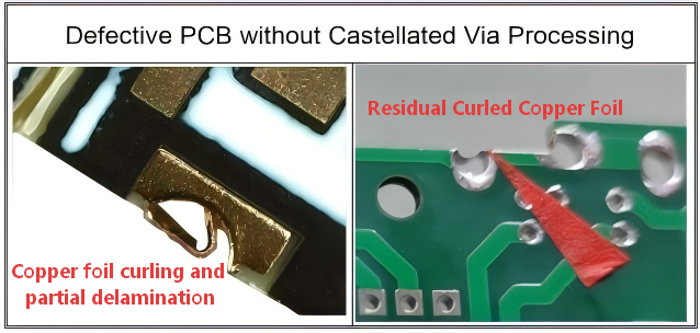
Quality Control and Process Challenges
Given the impact of via manufacturing on overall PCB performance, maintaining high quality is critical. Manufacturers implement several quality control measures:
- Microscopic Inspection: Operators use Automated Optical Inspection (AOI) systems to check plating quality and verify that vias comply with design specifications.
- Electrical Testing: Conductivity testing verifies that plated areas possess the required electrical characteristics, such as controlled impedance and minimum resistance.
- Dimensional Accuracy: Regular measurements ensure that drilled and plated areas meet design tolerances. Any deviation can affect component placement and signal integrity.
Although the castellated via process offers numerous advantages, it also presents several challenges. These challenges include ensuring consistent plating thickness, preventing over-plating in unintended areas, and controlling thermal stress throughout the manufacturing cycle. Overcoming these challenges requires a robust process control framework and continuous monitoring throughout production.
PCB Castellated Via Design Guidelines
To maximize the benefits of castellated via technology, designers must follow a series of best practices and design guidelines. These recommendations help ensure that the final PCB meets the required performance standards while avoiding common pitfalls.
- Drill Size and Tolerances: Ensure that drill sizes are compatible with the intended plating process. Precise drilling is critical for achieving consistent results.
- Plating Thickness: Determine the optimal plating thickness for the castellated vias based on the application’s electrical and mechanical requirements. Plating that is too thin may compromise conductivity, while plating that is too thick may lead to manufacturing challenges.
- Layer Stackup: Carefully plan the PCB’s layer configuration. The selective plating process must be compatible with the overall stackup design to maintain proper interconnectivity.
- Thermal Management: Consider the PCB’s thermal distribution, particularly in high-power applications. An appropriate via design aids in heat dissipation and reduces thermal stress on critical components.
- Signal Routing: Optimize the layout to minimize interference and ensure that vias do not introduce unwanted parasitic elements that could compromise signal integrity.
Future Trends and Innovations
As the demand for high-density, high-performance PCBs continues to grow, innovations in via-in-hole technology are also expected to evolve.
- Advanced Plating Technologies: New chemical and physical deposition methods can provide better control over selective plating, thereby further improving the reliability and performance of via-in-holes.
- Integrating with 3D PCB Design: Modern PCBs are evolving toward three-dimensional structures, and designers can combine castellated via technology with 3D interconnects to develop more compact, high-efficiency layouts.
- Enhanced Simulation Capabilities: Improvements in simulation tools will enable designers to more accurately simulate via-in-hole behavior, thereby optimizing designs and reducing manufacturing errors.
- Focus on Sustainability: With the growing emphasis on sustainable manufacturing practices, future innovations may focus on reducing material waste and energy consumption during the via-in-hole production process.
Summary
Castellated via technology represents a major innovation in PCB design, uniquely combining enhanced electrical performance, cost-effectiveness, and design flexibility. Through selective electroplating of drilled holes, manufacturers can create customized interlayer connections to meet the stringent requirements of modern electronic applications. The process involves advanced drilling and electroplating techniques, rigorous quality control, and careful consideration of design parameters.
For engineers and B2B professionals, understanding the complexities of via-in-hole technology is essential to fully harness its potential. By adhering to best practices and staying abreast of emerging trends, designers can optimize their PCB layouts to achieve superior signal integrity, improved thermal management, and enhanced overall performance. As the electronics industry continues to push the boundaries of innovation, via-in-hole technology will undoubtedly play a pivotal role in shaping the future of PCB manufacturing.
In summary, the adoption of castellated via technology on PCBs is not merely a manufacturing nuance but a strategic design choice that can significantly enhance performance and cost-effectiveness. Through careful planning, effective collaboration, and adherence to best practices, companies can leverage this technology to deliver reliable, high-performance products in a highly competitive market.


