What is PCB Reverse Engineering?
PCB reverse engineering refers to the professional process of reverse-engineering a PCB, schematic, and BOM (Bill of Materials) when only a physical PCBA (Printed Circuit Board Assembly) board is available. Simply put, the technical process of PCB reverse engineering involves the following key stages:
- First, scan the circuit board to be reverse-engineered and record the detailed component locations and parameters.
- Remove the components to create a complete bill of materials (BOM) and arrange for component procurement.
- For blank PCBs after component removal, scan them into high-resolution images and process them with professional PCB reverse engineering software to reconstruct the PCB layout file.
- Send the reconstructed PCB layout file to a PCB manufacturer for production.
- After we manufacture the PCB, we solder the procured components onto the finished board.
- Conduct circuit board testing and debugging to ensure the reverse-engineered PCB functions consistently with the original.
Detailed Steps for PCB Reverse Engineering (PCB Cloning)
Step 1: Scan the PCB Image (Prepare for PCB Reverse Engineering)
Step 2: Disassemble the Board (Critical for PCB Reverse Engineering Accuracy)
Remove all components from the PCB and clean the solder from the pad holes to avoid interfering with subsequent PCB reverse steps.
Clean the PCB thoroughly with alcohol or professional PCB cleaner, then place it in a scanner (a multifunction printer with scanning capabilities is sufficient).
Open the built-in scanning software (e.g., Windows 10 scanning tool), set the scan format and resolution (recommended: 1200 DPI or higher; image format: BMP) to ensure a clear image for PCB reverse analysis.
Scan the side with the silkscreen, save the file, and print it out for future reference during the PCB reverse process.
Important Note: When disassembling the board, pay close attention to the polarity and orientation of the components—this is crucial for accurate PCB reverse and subsequent assembly.
Step 3: Create a BOM (Bill of Materials) for PCB Reverse Engineering.
Refer to the circuit board image from Step 1 to record the model numbers, parameters, and locations of all components on paper. Focus on the orientation of diodes and transistors, as well as the notch direction of ICs. Use this information to create a detailed BOM table, which is essential for component procurement and successful PCB reverse engineering.
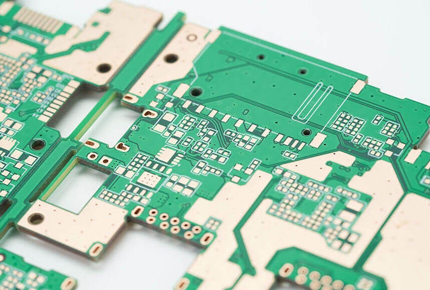
Step 4: Sanding the Board (Reveal Copper Traces for PCB Reverse)
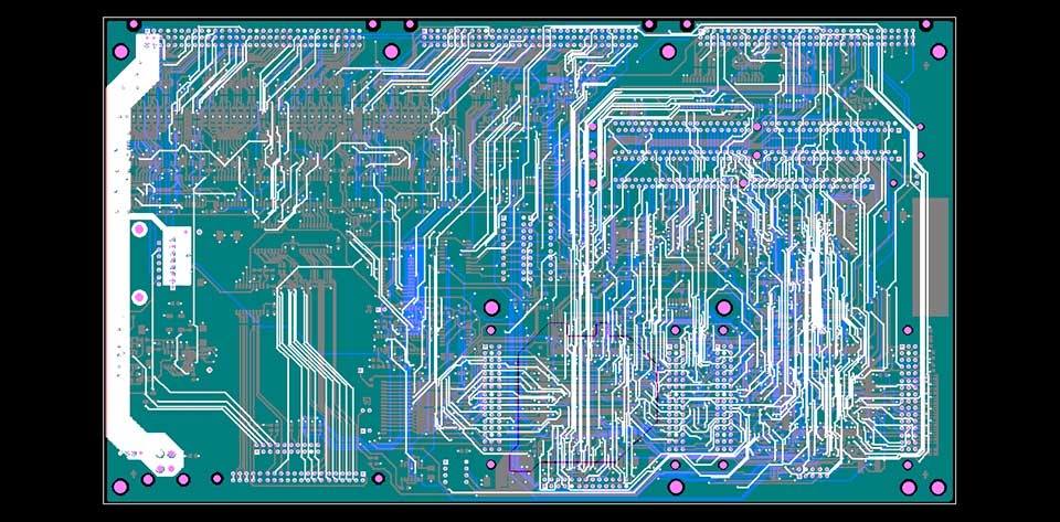
Use sandpaper to thoroughly sand off the ink (solder mask) from the top and bottom layers of the PCB until the copper surface shines. This step exposes the copper traces, which is critical for accurate PCB reverse engineering routing.
Place the sanded PCB in the scanner and scan both sides. Note: Ensure the PCB is positioned perfectly straight and level in the scanner; otherwise, the scanned image will be skewed, making subsequent image adjustments and PCB reverse work difficult. Save the scanned files for the next step.
Step 5: Image Editing (Optimize for PCB Reverse Software)
Open the scanned images in Photoshop (or other image editing software).
Adjust the canvas’s contrast and brightness to ensure a strong contrast between the copper-coated and non-copper-coated areas—this helps the PCB reverse software accurately identify traces.
Check whether the copper lines are clear; if not, repeat the adjustment step. If clear, save the images as color BMP files named TOP.BMP (top layer) and BOT.BMP (bottom layer).
If any issues are found in the graphics (e.g., blurred traces), use Photoshop to repair and correct them to avoid errors in the PCB reverse process.
Step 6: Image Alignment (Ensure PCB Reverse Precision)
Compare the scanned top and bottom layer images. If their positions largely overlap, it indicates that the previous steps were performed correctly. If there is a deviation, repeat Step 5 to adjust the images—accurate alignment is key to successful PCB reverse engineering.
Step 7: Package Creation and Trace Routing (Core of PCB Reverse)
Launch the professional PCB reverse engineering software. From the File menu, import the scanned PCB images.
For a two-layer board, import the top layer BMP image into the software and place it on the corresponding layer. Then, place components (using the BOM as a reference) and route traces for both the TOP and BOTTOM layers, replicating the original PCB’s circuit connections during the PCB reverse engineering process.
Step 8: Exporting the PCB File (Finalize PCB Reverse Output)
Once most of the design work is complete, export the file and save it in .pcb format—this file is the core output of the PCB reverse engineering process and will be used for PCB manufacturing.
Step 9: Post-processing and Optimization (Refine PCB Reverse Results)
Import the exported .pcb file into EDA (Electronic Design Automation) software for optimization. We recommend using Altium Designer 19 to: Optimize the PCB layout for better performance. Perform DRC (Design Rule Check) to ensure compliance with manufacturing standards.
Step 10: Generate the final PCB output file (e.g., Gerber files) for production.
At this point, the two-layer PCB reverse engineering (PCB cloning) process is successfully completed!
Methods for Multilayer PCB Reverse Engineering (Multilayer Cloning)
Most engineers feel intimidated by multilayer PCB reverse engineering, but we can simplify its core principle: Cloning a 4-layer PCB equals cloning two double-sided PCBs, and cloning a 6-layer PCB equals cloning three double-sided PCBs. The main challenge of multilayer PCB reverse engineering is that the internal traces are invisible, so the key is to separate the layers to reveal these hidden traces.
Layer Separation Method for Multilayer PCB Reverse
There are various methods for delaminating PCBs (e.g., chemical etching and knife peeling), but these can easily cause over-delamination and data loss. Based on industry experience, sanding with sandpaper is the most accurate, economical, and widely used method for multilayer PCB reverse engineering.
Sanding Steps for Multilayer PCB Reverse:
After tracing the top and bottom layers of the PCB (as per the two-layer PCB reverse steps), use sandpaper to grind away the surface layer to reveal the inner layers. Use ordinary sandpaper (available at hardware stores). Lay the PCB flat, hold the sandpaper down, and rub it evenly across the PCB (for small boards, lay the sandpaper flat and rub the PCB against it with your finger). The key is to keep the PCB flat to ensure even sanding—this avoids damaging the internal traces during the multilayer PCB reverse process.
The silkscreen and solder mask usually come off with a single wipe, but the copper traces and copper foil require several firm wipes. The time required depends on the board size: a small Bluetooth board can be sanded in a few minutes, while a memory module takes about 10–15 minutes. Applying moderate force can reduce sanding time without damaging the board.
Sanding is not technically difficult—it is just a bit tedious and requires some physical effort. There is no need to worry about sanding through the board or cutting your fingers with proper operation, making it ideal for multilayer PCB reverse engineering.
PCB Layout Review for PCB Reverse Engineering
After completing the PCB reverse engineering layout, a thorough review is essential to ensure the layout is reasonable, meets manufacturing requirements, and functions reliably. Evaluate the layout from the following aspects, which are critical for the success of PCB reverse engineering:
Routing Reasonableness
Does the system layout ensure reasonable or optimal routing? Does it guarantee reliable routing and the reliability of circuit operation? When reviewing the PCB reverse layout, you need to have a comprehensive understanding and plan for signal paths, as well as power and ground networks.
Dimensional and Process Compliance
Do the PCB dimensions match those on the manufacturing drawings? Do they meet PCB manufacturing process requirements? Are there any behavioral markers (e.g., alignment notches)? This requires special attention in PCB reverse engineering. While many PCB circuit layouts and routings are designed beautifully and logically, the precise positioning of connectors is often overlooked—this can result in circuits that cannot interface with other circuits, rendering the PCB’s rework ineffective.
2D/3D Component Conflict Check
Are there any conflicts between components in two-dimensional (footprint overlap) and three-dimensional (height interference) space? Pay attention to the actual dimensions of components, particularly their height. For components that require soldering, the height generally should not exceed 3 mm to avoid assembly issues after PCB reverse engineering.
Component Layout Order & Density
Check whether the component layout is orderly and evenly spaced, with components arranged neatly and all placements completed. When placing components during PCB reverse engineering, consider not only signal paths, signal types, and areas requiring attention or protection, but also the overall density of the layout to ensure uniform spacing and ease of assembly.
Maintainability & Serviceability
Verify that frequently replaced components can be easily swapped out and that insertion into the board is convenient. Ensure that the replacement and connection of frequently replaced components are both convenient and reliable—this is an often-overlooked detail in PCB reverse engineering, but critical for practical use.