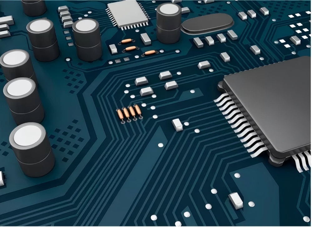
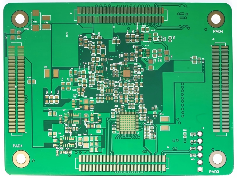
Engineers and technicians cannot ignore exposed copper on circuit boards—a common yet critical issue—during the manufacturing and maintenance of electronic devices. It not only affects the electrical characteristics and reliability of the circuit board but can also compromise the overall quality of the product. This article provides an in-depth discussion of the causes, impacts, and solutions for exposed copper on PCBs, offering targeted solutions and preventive measures to help electronic engineers and hobbyists quickly address such issues.
I. Analysis of the Causes of Exposed Copper on PCBs
(1) Design Defects
Inadequate Solder Mask Design: During the PCB design phase, inaccuracies or oversights in solder mask design can result in portions of the copper surface not being effectively covered. (How to Use Solder Mask on PCBs)
Excessive Open Areas: Excessive open areas in the routing design may lead to uneven distribution of plating current, affecting the uniformity of the copper layer.
(2) Manufacturing Process Defects
Uneven Solder Mask Coating: In PCB manufacturing, the solder mask application process directly impacts coverage. Insufficient coating thickness, trapped bubbles, or incomplete curing leave parts of the copper foil uncovered, leading to gradual exposure during later use.
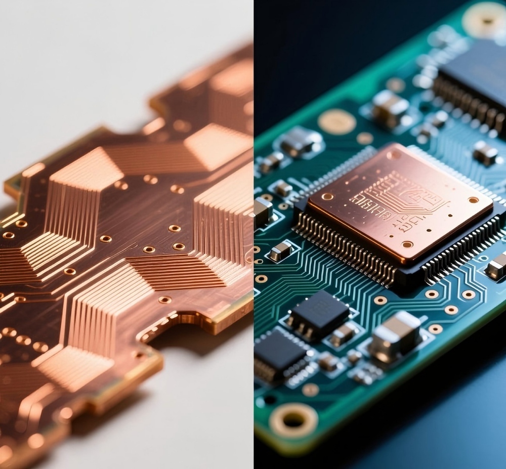
Over-etching: Etching is critical for removing excess copper foil from circuit boards, but excessive etching time or overly concentrated etchant can etch away the copper foil that should remain. This is especially problematic in high-density boards, where trace spacing is extremely narrow; even small etching deviations expose copper at trace edges and impair circuit function.
(3) Material Factors
Substrate and Copper Foil Quality: Using low-quality substrates or copper-clad laminates can easily result in poor adhesion of the copper layer, making it prone to peeling off.
(4) Improper Use and Maintenance
Mechanical Damage: External impacts, compression, or bending during installation, disassembly, or transportation can damage the surface solder mask of the circuit board and expose the copper foil. For example, in laptop drop incidents, violent vibrations can cause the solder mask to crack, resulting in exposed copper.
Environmental Corrosion: Prolonged exposure to humid, acidic, alkaline, or high-salt-fog environments causes the solder mask on the PCB surface to gradually age and peel off, leaving the copper foil unprotected. In coastal regions, where the air has a high salt content, copper exposure on PCBs is more common than in inland areas.
II. Hazards of Exposed Copper on Circuit Boards
(1) Degradation of Electrical Performance
In areas where copper foil is exposed, it comes into direct contact with the air, making it highly susceptible to oxidation. This forms a layer of copper oxide with poor conductivity, leading to increased circuit resistance and unstable signal transmission. If exposed copper occurs on high-frequency signal lines, it can also cause signal attenuation and interference, severely affecting the device’s communication and computational performance.
(2) Increased Risk of Short Circuits
When exposed copper areas come into contact with adjacent circuits or the ground plane, or when metal debris or conductive liquids adhere to them, short circuits may occur. In power supply circuits, short circuits can cause components to burn out and may even lead to serious accidents such as fires.
(3) Reduced Service Life
Oxidized copper foil continues to corrode, causing the traces to gradually thin and break, which leads to circuit board failure. Even without a short circuit, exposed copper accelerates the aging process of the circuit board, shortening the overall service life of the electronic device.
III. Methods for Addressing Exposed Copper on Circuit Boards
(1) Repairing Minor Exposed Copper
Repair with a Solder Mask Pen: For small, non-critical areas of exposed copper, a specialized solder mask pen can be used for repair. First, clean the exposed copper surface to remove the oxide layer and impurities. Then, apply the solder mask pen evenly over the exposed area. Once it dries and cures, it will re-form an insulating protective layer. Solder mask pens are easy to use, but care must be taken to ensure even application thickness to avoid new bubbles or thickness variations.
Applying Insulating Varnish: If a solder mask pen is unavailable, insulating varnish can be used for repair. Insulating varnish offers excellent electrical insulation properties and adhesion, effectively sealing off the copper foil from the air. Use a fine-bristled brush to ensure a thin, even coat. After drying, check the insulation effectiveness and reapply if necessary.
(2) Treatment for Moderate Copper Exposure
Local Application of Insulating Tape: For slightly larger or more complex areas of copper exposure, cover them with high-temperature-resistant polyimide tape that offers excellent insulation. First, clean the exposed copper surface, then cut the tape to the appropriate size and precisely cover the exposed area, ensuring the tape edges adhere tightly to the circuit board to prevent moisture and contaminants from penetrating.
Re-printing the Solder Mask: If the circuit board has multiple exposed copper areas or requires higher insulation for exposed regions, we can reapply the solder mask. This method uses specialized equipment and processes, so manufacturers or professional repair facilities typically perform this repair. Technicians will first clean and pretreat the circuit board, then reapply the solder mask through processes such as screen printing, exposure, and development.
(3) Severe Exposed Copper Repair
When exposed copper causes circuit breaks or severely impairs circuit functionality, circuit repair is necessary. For finer circuits, conductive silver paste or fine copper wire can be used for repair. First, carefully apply conductive silver paste to the break; once it dries and cures, it forms a conductive path. Alternatively, solder fine copper wire to both ends of the broken circuit to restore the connection. If the circuit damage is severe, it may be necessary to replace a section of the PCB or the entire board.
IV. Preventive Measures for Exposed Copper on Circuit Boards
(1) Optimizing Production Processes
Strictly control the quality of the solder mask: During circuit board production, use high-precision coating equipment to ensure that the solder mask ink uniformly and completely covers the copper foil surface. Strengthen production process monitoring, regularly inspect indicators such as solder mask thickness and curing degree, and adjust process parameters on time.
Precise Etching Process: In accordance with PCB design requirements, precisely control the concentration, temperature, and duration of the etching solution. Utilize advanced etching equipment and processes, such as spray etching and electrolytic etching, to minimize etching deviations and prevent over-etching.
(2) Proper Use and Maintenance
Enhanced Protective Measures: During PCB installation, removal, and transportation, implement anti-vibration, anti-compression, and anti-static measures. Use dedicated packaging boxes and tools to prevent mechanical damage to the PCBs. For equipment exposed to harsh environments over extended periods, install protective enclosures or perform potting.
Regular Maintenance Inspections: Establish a regular maintenance schedule to inspect the PCB surface for damage, exposed copper, and other issues. Clean the circuit boards promptly to remove dust, oil, and other contaminants. Address any issues immediately upon discovery to prevent them from worsening.
Summary:
While exposed copper on circuit boards is common, a thorough understanding of its causes, the application of scientific treatment methods, and the implementation of preventive measures can effectively prevent various faults caused by copper exposure and ensure the stable operation of electronic equipment. Whether through strict control during production or careful maintenance during use, these steps are key to reducing exposed copper issues and enhancing the reliability of circuit boards.


