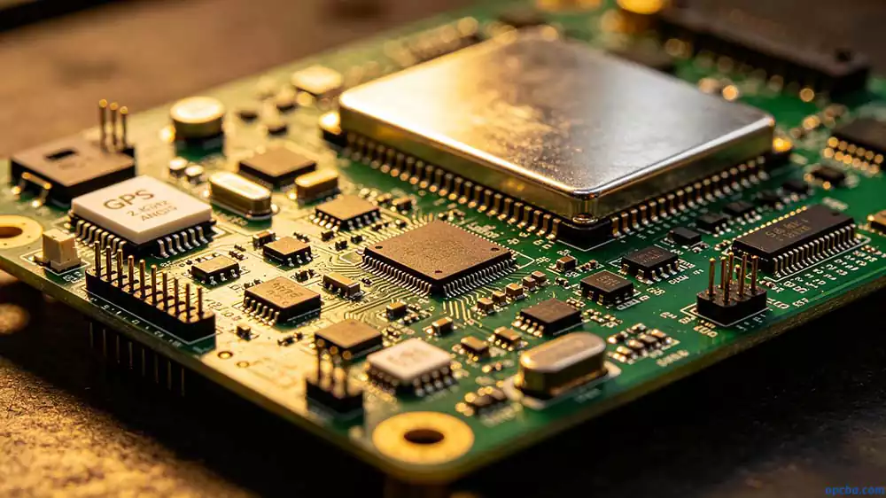
When a UAV antenna fails to achieve the expected range or exhibits unstable signal reception, the root cause is often not the antenna element itself—it’s the PCB it’s built on. Many engineers treat the antenna as a standalone component, selecting a ready-made module and assuming it will perform as specified once mounted on the drone. In practice, the PCB substrate, copper trace dimensions, ground plane configuration, and even the placement of nearby components all directly determine whether that antenna resonates at the correct frequency. If you’re new to core PCB concepts and terminology, start with our foundational overview: Printed Circuit Board(PCB)
This guide approaches uav antenna design from the PCB engineer’s perspective—not antenna theory, not system-level RF architecture, but the physical implementation that makes or breaks real-world performance. For a full foundational framework covering general RF antenna principles and PCB design methodology, see our comprehensive guide: RF Antenna Design and PCB Design
1. Why UAV Antenna Performance Is PCB-Dependent
An antenna is not a separate device plugged into a PCB. For microstrip patch antennas—the most common type used in UAV applications—the PCB is the antenna. The patch is a copper trace on the board; the ground plane is another layer; the substrate between them is the dielectric that determines resonant frequency.
Here’s what that means in practice:
- Resonant frequency is determined by the patch dimensions and the substrate’s dielectric constant (Dk). A 5% Dk deviation shifts the resonant frequency by roughly the same percentage.
- Bandwidth is influenced by substrate thickness and Dk. Thinner substrates yield narrower bandwidth.
- Gain and efficiency are affected by dielectric loss (Df) and copper surface roughness.
The common mistake: Designing the antenna in a simulation environment using ideal material parameters, then sending the PCB to a fab that uses a different batch of laminate with slightly different Dk. The board comes back, and the antenna is off-frequency by 50-100MHz—enough to kill the link budget entirely.
Engineer’s rule of thumb: Always design with the actual material parameters from your PCB manufacturer’s current batch, not the datasheet typical values.
2. UAV Antenna Types and Their PCB Implementation
Different antenna types impose different constraints on PCB design. Understanding these constraints upfront prevents late-stage redesigns.
Microstrip Patch Antennas
This is the workhorse of UAV communications. A rectangular or circular copper patch on the top layer, with a ground plane on the layer beneath. Key PCB considerations:
- Substrate thickness typically 0.2–0.8mm. Thicker substrates increase bandwidth but also increase weight.
- Feed line must be 50Ω matched. This means calculating trace width based on substrate Dk and thickness.
- The ground plane beneath the patch must be continuous—no splits, no voids in the projection area.
Dipole and Monopole Antennas
These can be implemented as PCB traces, often on the edge of the board. Key PCB considerations:
- The trace width affects the antenna’s impedance bandwidth—wider traces increase bandwidth but reduce radiation resistance.
- For monopoles, the ground plane size directly affects the radiation pattern. A ground plane that’s too small distorts the pattern.
Array Antennas
When a single element can’t provide enough gain or directivity, arrays are used. Key PCB considerations:
- The feeding network (power dividers, phase shifters) is entirely implemented on the PCB.
- Phase matching between elements requires precise trace length control—often within ±0.5mm at 5.8GHz.
- Mutual coupling between elements is affected by PCB material Dk and inter-element spacing.
Vivaldi and Horn Antennas
These are less common in PCB form but can be implemented using multilayer PCB techniques. Key PCB considerations:
- Require precision machining of the PCB substrate.
- Layer alignment becomes critical—misalignment of even 0.05mm affects the taper profile.
Bottom line: For 80% of UAV applications, a microstrip patch or printed dipole implemented directly on the main PCB is the most cost-effective and weight-efficient solution.
3. PCB Material Selection for UAV Antennas
Material selection is where many uav antenna projects succeed or fail. The choice isn’t simply “use the cheapest FR4” or “use Rogers for everything”—it depends on frequency, weight budget, and cost constraints.
Key Material Parameters
| Parameter | What It Affects | Why It Matters |
| Dk (Dielectric Constant) | Resonant frequency, trace dimensions | A ±0.2 Dk variation shifts frequency by ±3-5% |
| Df (Dissipation Factor) | Loss, efficiency | Higher Df = more signal loss = shorter range |
| Thickness tolerance | Impedance control | ±10% thickness = ±10% impedance variation |
| CTE (Coefficient of Thermal Expansion) | Dimensional stability | Affects frequency stability across temperature |
Frequency-Based Selection Guide
Below 3GHz (2.4GHz WiFi, 915MHz telemetry):
- Standard FR4 (Dk \4.2-4.6, Df \0.02) is acceptable for most applications.
- Use high-Tg FR4 (TG170+) for better dimensional stability.
- Trace width for 50Ω microstrip on 1.6mm FR4: approximately 3.0mm—wide enough to be practical.
3-10GHz (5.8GHz FPV, C-band radar):
- Low-loss materials are recommended. RO4350B (Dk 3.66, Df 0.004) is widely used.
- Alternative: Megtron 6 or Isola 370HR.
- Trace width for 50Ω on 0.508mm RO4350B: approximately 0.32mm.
Above 10GHz (millimeter-wave, 24GHz radar, 60GHz communication):
- High-frequency laminates required. RO3003, RO4000 series, or PTFE-based materials.
- Copper roughness becomes critical due to skin effect—smooth copper (VLP/RTF) is essential.
- Consider antenna-in-package (AiP) approaches where the antenna is integrated into the module package.
The Hybrid Approach
Full-board use of Rogers materials is expensive (3-5× FR4 cost). A practical compromise: use Rogers only in the antenna region, FR4 for the rest of the board. This requires:
- Controlled impedance transitions between the Rogers and FR4 sections.
- Careful management of the material interface (step in dielectric height).
- Board fabrication capability for mixed-material lamination.
What this looks like in practice: For a 5.8GHz FPV drone board, we typically specify RO4350B for the antenna feed section (approximately 10×15mm area) and standard FR4 for the rest. This keeps cost down while ensuring the antenna section has stable, low-loss performance.
4. UAV Antenna PCB Layout Guidelines
Layout is where theory meets reality. The following guidelines are based on real engineering practice, not textbook idealizations.
Antenna Placement
Rule 1: Keep the antenna away from board edges where possible. Edge placement increases detuning effects from nearby objects and makes the radiation pattern more susceptible to the drone’s airframe.
Rule 2: Maintain a keep-out area around the antenna. For microstrip patches, the keep-out area should extend at least one substrate thickness beyond the patch edges in all directions. No copper traces, no components, no vias in this zone.
Rule 3: Consider the drone’s airframe. Carbon fiber airframes are conductive and will detune antennas. If the antenna is mounted near carbon fiber, simulate with the airframe model included, or leave extra margin in the design.
Ground Plane Design
The ground plane beneath a microstrip patch antenna must be:
- Continuous: No slots, no splits, no voids in the projection area.
- Sufficiently large: At least 3× the patch dimensions in each direction.
- Low-impedance: Use multiple vias to connect ground planes on different layers.
A common failure: Routing a power trace through the ground plane underneath the antenna “because there was nowhere else to put it.” This splits the ground plane, changes the effective dielectric constant under the patch, and shifts the resonant frequency.
Feed Line Design
The feed line—typically a 50Ω microstrip line—connects the RF source to the antenna. Critical considerations:
- Impedance matching: Calculate trace width precisely based on the substrate’s actual Dk and thickness. Don’t rely on generic calculators—use the manufacturer’s measured parameters.
- Length: Keep the feed line as short as practical. Every millimeter of line adds loss and phase error.
- Bends: Avoid sharp 90° bends. Use mitered bends (45° corners with chamfer) to minimize impedance discontinuities.
- Via transitions: If the feed must transition between layers, use a grounded coplanar waveguide (GCPW) structure around the via to maintain 50Ω impedance.
Practical Trace Width Reference
For a 50Ω microstrip line on common UAV PCB materials:
| Substrate | Thickness | Dk | 50Ω Trace Width |
| FR4 | 0.8mm | 4.4 | ~1.5mm |
| FR4 | 1.6mm | 4.4 | ~3.0mm |
| RO4350B | 0.254mm | 3.66 | ~0.55mm |
| RO4350B | 0.508mm | 3.66 | ~0.32mm |
| RO3003 | 0.254mm | 3.00 | ~0.65mm |
5. Key Parameters and Tolerances in Manufacturing
Dielectric Constant Variation
The Dk value on a material datasheet is a typical value, not a guarantee. Actual Dk varies by:
- Batch-to-batch: ±0.1-0.2 for FR4, ±0.05 for Rogers.
- Frequency: Dk typically decreases slightly as frequency increases.
- Temperature: Dk changes with temperature (TCDk).
Engineering response: Design the antenna with a tuning stub or matching network that can be adjusted after board fabrication. This allows compensation for Dk variation without a full redesign.
Trace Width Tolerance
PCB fabrication has trace width tolerances. For a 0.32mm trace (typical for 50Ω on 0.508mm RO4350B), a ±0.03mm tolerance represents approximately ±10% impedance variation.
Engineering response: When designing the antenna, run simulations at the minimum and maximum trace widths (accounting for fab tolerance) to ensure the antenna still meets specifications across the full tolerance range.
Copper Surface Roughness
At frequencies above 10GHz, copper surface roughness significantly affects conductor loss due to skin effect. Smooth copper (VLP—very low profile, or RTF—reverse treated foil) is recommended for millimeter-wave designs.
6. Multi-Antenna Coexistence on UAV PCBs
A typical UAV carries multiple antennas: GPS/GNSS, 2.4GHz control link, 5.8GHz video downlink, and sometimes additional telemetry or radar antennas. These must coexist on the same PCB without mutual interference.
Isolation Strategies
Spatial separation: The most effective isolation method. Place antennas as far apart as physically possible on the board. A rule of thumb: separation of at least λ/4 at the lowest operating frequency.
Orthogonal polarization: Use different polarizations for different links. For example, use linear polarization for control and circular for video. This provides 10-20dB of additional isolation.
Frequency filtering: Add band-pass filters at the front end of each receiver to reject out-of-band signals from other transmitters.
Ground plane partitioning: In extreme cases, split the ground plane to isolate different RF sections—but be aware that this creates potential for ground loops and requires careful management of the single-point ground connection.
Placement Priority
When space is constrained (as it always is on a UAV), prioritize placement as follows:
- GPS antenna: Needs clear sky view, place on top of the airframe away from all other antennas.
- Control link antenna: Second priority, needs reliable omnidirectional coverage.
- Video link antenna: Can be placed on the bottom or side, as video link is often more directional.
7. Practical Design Checklist for UAV Antenna PCB
Use this checklist before sending your design to fabrication:
□ Material selection confirmed with PCB fab (actual Dk/Df values for current batch) □ 50Ω feed line impedance calculated with actual material parameters □ Trace width tolerance accounted for in simulation (±10% min/max) □ Keep-out area around antenna: ≥1× substrate thickness beyond patch edges □ Ground plane under antenna: continuous, no splits, ≥3× patch dimensions □ Feed line length minimized, bends mitered (no sharp 90°) □ Via transitions use GCPW structure to maintain 50Ω □ Multi-antenna isolation: separation ≥λ/4, polarization diversity where possible □ Tuning stub or matching network included for post-fab adjustment □ Copper surface finish specified (ENIG or ENEPIG preferred, HASL not recommended) □ PCB fab confirmed capability for specified trace width tolerance □ If hybrid material (Rogers+FR4): fab confirmed mixed-material lamination capability □ Weight estimate: antenna PCB section within UAV weight budget
Conclusion: Start Your UAV Antenna Design from the PCB Layer
The difference between a UAV that achieves its specified range and one that falls short by 30% is often not the antenna design itself—it’s the PCB implementation. Material selection, layout, ground plane integrity, and manufacturing tolerances all play decisive roles in whether the antenna performs as simulated.
For PCB engineers working on UAV projects, the key takeaway is this: treat the antenna as an integral part of the PCB, not an add-on component. Specify materials with the fab early. Design with tolerance in mind. Include tuning capability. And always—always—simulate with the actual parameters your manufacturer will use.
If you’re developing a UAV antenna PCB and need engineering review or fabrication support, send your design files to OPCBA. Our engineering team provides DFM review for antenna PCBs, material selection recommendations, and impedance-controlled fabrication—typically within 24 hours of receiving your Gerber files. For inquiries or to submit your design for a free manufacturability check, email us directly at sales@opcba.com.


