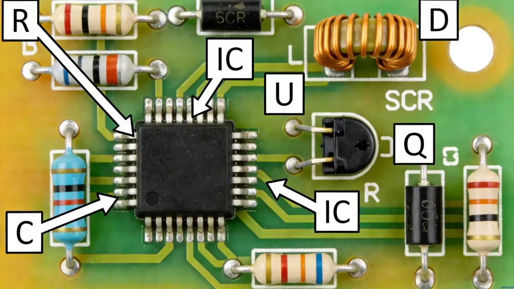
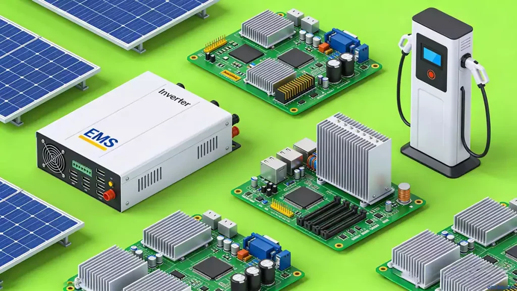
When a standard FR4 PCB fails under high power or extreme temperature, many engineers instinctively look for a “better PCB”—higher Tg, thicker copper, maybe a metal core. But in some applications, the problem isn’t the board’s construction; it’s the material itself. FR4 is an organic composite. It traps heat, expands with temperature, and degrades over time. Ceramic circuit boards are not an incremental improvement over FR4—they are a fundamentally different platform built on an inorganic, solid ceramic foundation. If you’re new to core PCB concepts and terminology, start with our foundational overview: Printed Circuit Board(PCB)
This guide approaches ceramic circuit boards from the PCB engineer’s perspective: what materials are available, how they’re manufactured, how to design with them, and—most importantly—when to choose them over conventional options.
1. What Is a Ceramic Circuit Board?
A ceramic circuit board is a printed circuit board that uses a ceramic material as the substrate instead of traditional organic laminates like FR4 or polyimide. The ceramic base serves as both the structural foundation and the electrical insulator, while copper circuitry is applied through various metallization processes.
The key distinction: In a conventional PCB, the substrate is a passive carrier. In a ceramic PCB, the substrate is an active participant in thermal management, mechanical stability, and electrical performance. The ceramic itself conducts heat, matches the thermal expansion of silicon chips, and maintains stable dielectric properties across extreme temperatures.
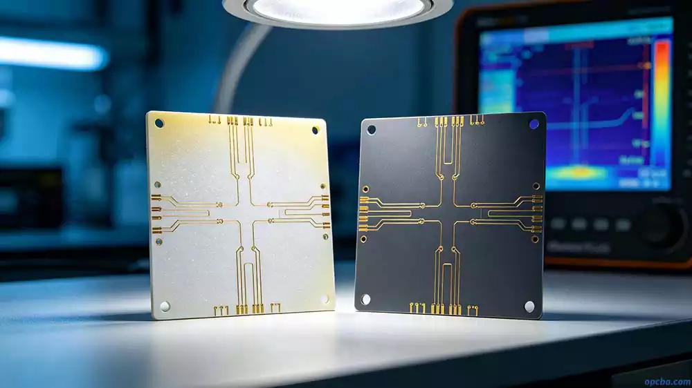
Common ceramic substrate materials include:
- Alumina (Al₂O₃) – the most widely used, cost-effective option
- Aluminum Nitride (AlN) – ultra-high thermal conductivity
- Beryllium Oxide (BeO) – highest thermal conductivity, but toxic
- Silicon Nitride (Si₃N₄) – high fracture toughness, ideal for automotive
2. Ceramic Substrate Materials Compared
Material selection is the first and most consequential decision in ceramic circuit board design. The choice determines thermal performance, mechanical reliability, cost, and manufacturability.
Alumina (Al₂O₃) – The Workhorse
Alumina is the most common ceramic substrate material, offering the best balance between performance and cost.
| Property | Value |
|---|---|
| Thermal Conductivity | 15–35 W/m·K |
| Max Operating Temperature | >800°C |
| Dielectric Strength | Up to 28 kV/mm |
| Relative Cost | Low |
| Typical Purity | 96% or 99.6% |
When to choose Al₂O₃: General high-power applications, LED arrays, voltage sensors, inverters, and any project where cost sensitivity exists alongside performance needs. For a full deep dive into specifications, processing details, and use cases of this mainstream ceramic substrate, refer to our dedicated guide: Alumina ceramic PCB
Aluminum Nitride (AlN) – The High-Performance Choice
AlN is the premium choice for extreme thermal demands. Its thermal conductivity approaches that of pure aluminum—an order of magnitude higher than alumina.
| Property | Value |
|---|---|
| Thermal Conductivity | 170–320 W/m·K |
| Max Operating Temperature | >800°C |
| CTE Match to Silicon | Excellent |
| Relative Cost | High |
When to choose AlN: High-power laser diodes, EV power inverters, RF power amplifiers, IGBT modules, and any application where immediate heat extraction from the junction is critical.
Beryllium Oxide (BeO) – The Specialist
BeO offers the highest thermal conductivity among ceramic substrates (280–300 W/m·K). However, its dust is toxic, limiting its use to specialized applications where the performance justifies the handling precautions.
When to choose BeO: Aerospace, defense, and high-power RF applications where maximum thermal performance is non-negotiable and proper safety protocols are in place.
Silicon Nitride (Si₃N₄) – The Tough One
Si₃N₄ has lower thermal conductivity than AlN but significantly higher fracture toughness and bending strength.
When to choose Si₃N₄: Automotive applications where mechanical shock and vibration resistance are as important as thermal performance.
Material Selection Quick Reference
| Material | Thermal Conductivity | Cost | Toughness | Best For |
|---|---|---|---|---|
| Al₂O₃ | 15–35 W/mK | Low | Moderate | General high-power, cost-sensitive |
| AlN | 170–320 W/mK | High | Moderate | Extreme heat, power modules |
| BeO | 280–300 W/mK | Very High | Moderate | Aerospace/defense, max performance |
| Si₃N₄ | 80–120 W/mK | High | High | Automotive, shock-prone environments |
3. Manufacturing Processes: Which One to Choose?
Ceramic circuit boards can be manufactured through several different processes. The choice of process affects line width capability, copper thickness, cost, and whether plated through-holes are possible.
DPC (Direct Plated Copper)
DPC uses a magnetron sputtering process to deposit a thin copper seed layer on the ceramic substrate, followed by photolithography and electroplating to build up the circuit pattern.
Key advantages:
- Fine line capability: 20–30μm line width
- High alignment accuracy: pattern positioning typically within ±15μm
- Surface roughness < 0.5μm, suitable for wire bonding
- Process temperature below 300°C avoids material degradation
- Plated through-holes are possible
Limitations: Copper thickness is limited; bonding strength between metal and ceramic is lower than DBC.
Best for: LiDAR, laser diodes, RF devices, sensors, precision cooling chips, and applications requiring fine features.
DBC (Direct Bonded Copper)
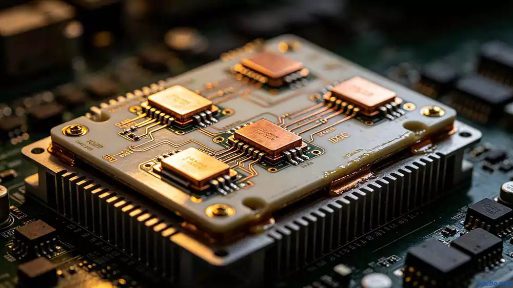
DBC bonds copper directly to the ceramic surface using a high-temperature oxidation process. The copper is typically thicker than DPC—140μm (4oz) to 350μm (10oz).
Key advantages:
- High copper thickness for high current carrying capacity
- Strong metallurgical bond between copper and ceramic
Limitations: Coarser line widths due to etch tolerances; plated through-holes are not available with standard DBC.
Best for: High-power IGBT modules, power electronics, and applications requiring heavy copper.
LTCC (Low-Temperature Co-Fired Ceramic) and HTCC (High-Temperature Co-Fired Ceramic)
LTCC and HTCC involve stacking multiple layers of ceramic green tape, printing conductor patterns on each layer, and co-firing the entire stack.
Key advantages:
- True multilayer capability (unlike single/double-layer DPC/DBC)
- Embedded passive components possible
- Compact, integrated RF circuits and SiP solutions
Limitations: Higher cost; longer lead times.
Best for: RF modules, wireless communication, satellite systems, and complex multilayer designs.
Thick Film vs Thin Film
| Process | Line Width | Copper Thickness | Cost | Applications |
|---|---|---|---|---|
| Thick Film | >100μm | 10–50μm | Lower | General purpose, resistors |
| Thin Film | 20–30μm | <10μm | Higher | Precision RF, wire bonding |
Process Selection Decision Guide
Choosing the right manufacturing process depends on your specific design requirements. Follow this logical sequence:
Step 1: Evaluate line width and via requirements
If your design requires fine-line circuitry (<50μm) and plated through-holes (PTH) are mandatory → choose DPC (Direct Plated Copper). DPC is currently the only ceramic PCB process that simultaneously delivers high-precision trace routing and plated through-hole capability.
If your design requires high current handling (>50A) and thick copper (≥140μm / 4oz) → choose DBC (Direct Bonded Copper). DBC supports copper thickness up to 350μm (10oz), making it suitable for power modules.
Step 2: Assess whether multilayer integration is needed
If a single-layer or double-sided board cannot accommodate your routing density and you genuinely require 3 or more layers → choose LTCC or HTCC. Note: this is the only ceramic PCB process route that supports true multilayer integration, but cost and lead times are correspondingly higher.
Step 3: Confirm cost and precision targets
If none of the above special requirements apply, and you only need standard circuit routing on a ceramic substrate → choose Thick Film (lowest cost, line width >100μm) or Thin Film (higher precision, line width 20–30μm, suitable for RF and wire bonding applications).
4. Ceramic PCB Design Guidelines
Designing for ceramic circuit boards is different from designing for FR4. The material’s brittleness, thermal expansion characteristics, and manufacturing constraints impose specific rules.
Layer Count: Single vs Double vs Multilayer
Most ceramic PCB manufacturers recommend single-layer or double-sided designs. While 4-layer ceramic PCBs are technically possible, they are prone to cracking during lamination.
Engineering judgment: If your design requires more than 2 layers, seriously consider whether LTCC is the right approach, or whether you can split the design across multiple boards.
Trace Width and Spacing
Trace dimensions must account for both current carrying capacity and mechanical stress.
| Copper Thickness | Recommended Min Trace Width | Recommended Min Spacing |
|---|---|---|
| 1oz (35μm) | 0.2mm | 0.2mm |
| 2oz (70μm) | 0.3mm | 0.3mm |
| 3oz (105μm) | 0.4mm | 0.4mm |
Additional rules:
- For currents >5A, use wider traces or parallel traces
- Low-voltage signals (≤30V): spacing ≥0.2mm
- High-voltage signals (≥100V): spacing ≥0.5mm
- Avoid sharp 90° corners—use radiused bends to reduce stress concentration
Edge Clearance
Maintain adequate margin between copper traces and the board edge:
| Copper Thickness | Minimum Edge Margin |
|---|---|
| 1oz | 0.3mm |
| 2oz | 0.4mm |
| 3oz | 0.5mm |
Via Design
- Minimum via diameter: 0.15mm (larger diameters >0.5mm are more cost-effective)
- DPC supports plated through-holes; standard DBC does not
- More vias increase cost—use them judiciously
Panel Size Limitations
Ceramic substrates are produced in smaller panel sizes than FR4.
- Typical master panel: 115 × 115mm
- Maximum usable area: approximately 160 × 240mm
- Maximum recommended size for reliable manufacturing: 138 × 190mm
- Check with your manufacturer for their specific panel capabilities and any panelization options
Practical constraint: If your board’s larger dimension exceeds 190mm, or if both dimensions exceed 140mm, discuss panelization options with your manufacturer early in the design phase. For standard panels, many fabs can accommodate boards up to 115mm × 115mm without panelization.
Surface Finish Options
Ceramic PCBs support the same surface finishes as conventional PCBs:
- ENIG (Electroless Nickel Immersion Gold)
- ENEPIG (Electroless Nickel Electroless Palladium Immersion Gold)
- EPIG
- Immersion Silver / Immersion Tin
- OSP
Note: Solder mask is often not applied to ceramic PCBs because most boards operate at temperatures (>200°C) that exceed the rating of standard soldermasks.
5. Ceramic PCB vs FR4 vs Metal Core: When to Use Which
This is the question engineers ask most often. Here’s the data-driven answer.
Thermal Performance Comparison
| Material | Thermal Conductivity | Max Operating Temp |
|---|---|---|
| FR4 | 0.3–0.5 W/mK | ~130–170°C (Tg dependent) |
| Metal Core (IMS) | 1–5 W/mK (through dielectric) | ~150°C |
| Al₂O₃ Ceramic | 15–35 W/mK | >800°C |
| AlN Ceramic | 170–320 W/mK | >800°C |
The critical difference: In a metal-core PCB, heat must pass through an insulating dielectric layer (3–6 W/mK) between the circuit and the metal base. In a ceramic PCB, the ceramic itself is both the insulator and the thermal conductor—there is no intermediate barrier. This can reduce junction-to-base thermal resistance by 30–50% compared to MCPCBs.
CTE Matching
FR4 has a CTE of approximately 14–17 ppm/°C, while silicon is ~3 ppm/°C. This mismatch creates thermal stress during temperature cycling, a leading cause of failure in high-power electronics. Ceramic substrates have CTE closely matched to silicon (AlN: ~4.5 ppm/°C), dramatically reducing this stress.
Decision Framework
Step 1: Is heat the primary constraint? If your application doesn’t generate significant heat, FR4 will suffice—there’s no need to increase cost. If heat is a real concern, proceed to the next step.
Step 2: What is the power density? For moderate power (<5W/cm²), consider MCPCB—lower cost than ceramic. For high power (5–20W/cm²), Al₂O₃ ceramic is recommended. For extreme power (>20W/cm²), AlN ceramic is required for effective heat dissipation.
Step 3: Is mechanical shock a significant factor? If the board will be installed in a high-vibration environment (e.g., automotive chassis, engine compartment), Si₃N₄ ceramic is the more reliable choice. If there are no special shock requirements, standard Al₂O₃ or AlN will suffice.
Step 4: Are board dimensions compatible with ceramic manufacturing? Ceramic substrate panels are smaller than standard FR4 panels. Most manufacturers support boards up to approximately 115mm × 115mm without panelization. If your board’s larger dimension exceeds 190mm, or if both dimensions exceed 140mm, discuss panelization options with your manufacturer early in the design phase—large ceramics are prone to cracking and may not be feasible as a single piece.
6. Common Applications and Real-World Cases
Ceramic circuit boards are used wherever conventional PCBs reach their thermal, mechanical, or electrical limits.
High-Power LED Lighting
High-brightness LEDs generate significant heat that must be extracted to maintain lumen output and lifespan. Ceramic PCBs, particularly Al₂O₃, are widely used in automotive headlights, street lighting, and stadium lights.
Why ceramic works: The direct thermal path from LED junction to heatsink through the ceramic substrate minimizes junction temperature rise, extending LED life from thousands to tens of thousands of hours.
Power Modules (IGBT, MOSFET)
IGBT modules and power amplifiers handle high currents and generate massive heat. DBC ceramic substrates with thick copper (up to 10oz) are the industry standard for these applications.
Why ceramic works: The combination of high thermal conductivity and CTE matching to silicon prevents solder fatigue and extends module lifetime under thermal cycling.
RF and Microwave Systems
Ceramic substrates have low dielectric loss (Df) and stable dielectric constants (Dk), making them ideal for high-frequency signal integrity. LTCC technology is used to create compact, integrated RF circuits with embedded passive components.
Applications: Base station amplifiers, radar modules, satellite communications, and 5G infrastructure.
Automotive Electronics
Under-hood electronics must survive extreme temperatures, vibration, and thermal cycling. Si₃N₄ ceramic substrates, with their high fracture toughness, are increasingly used in engine control systems and powertrain modules.
Aerospace and Defense
Mission-critical systems require reliability, airtightness, and stability across extreme temperature variations. BeO and AlN ceramic PCBs are used in satellite transceivers, radar systems, and avionics.
7. Ceramic PCB Design Checklist
Use this checklist before finalizing your ceramic PCB design:
□ Material selection confirmed: Al₂O₃ / AlN / BeO / Si₃N₄
□ Thermal conductivity requirement matched to material choice
□ Board dimensions compatible with manufacturer’s panel size limits:
– Most fabs support ≤115mm × 115mm without panelization
– If board exceeds 138mm × 190mm, discuss feasibility early
□ Layer count: single/double layer preferred; multilayer only with LTCC/HTCC
□ Trace width/spacing verified against copper thickness
□ Edge clearance: ≥0.3mm for 1oz, ≥0.4mm for 2oz, ≥0.5mm for 3oz
□ Sharp 90° corners avoided; radiused bends used instead
□ Via diameter: ≥0.15mm (≥0.5mm preferred for cost)
□ Via type confirmed compatible with chosen process (DPC supports PTH; DBC does not)
□ Surface finish selected: ENIG / ENEPIG / Immersion Ag / Immersion Sn / OSP
□ Solder mask: confirmed not required (or high-temp mask specified)
□ CTE mismatch considered for assembled components
□ Panelization discussed with manufacturer if board size > standard
□ DFM review requested from PCB manufacturer
Conclusion: Start Your Ceramic Circuit Board Design with the Right Foundation
Ceramic circuit boards are not a drop-in replacement for FR4. They require different material selection criteria, different design rules, and different manufacturing considerations. But when the application demands high power, extreme temperature, or mission-critical reliability, ceramics offer performance that no organic substrate can match.
The key to a successful ceramic PCB project is making the right decisions early—material, process, and design rules—before committing to fabrication. The differences between Al₂O₃ and AlN, between DPC and DBC, between single-layer and multilayer, all have profound implications for cost, performance, and manufacturability.
If you’re developing a ceramic circuit board and need engineering review or fabrication support, send your design files to OPCBA. Our engineering team provides DFM review for ceramic PCBs, material selection recommendations, and process-specific design guidance—typically within 24 hours of receiving your Gerber files. For inquiries or to submit your design for a free manufacturability check, email us directly at sales@opcba.com.