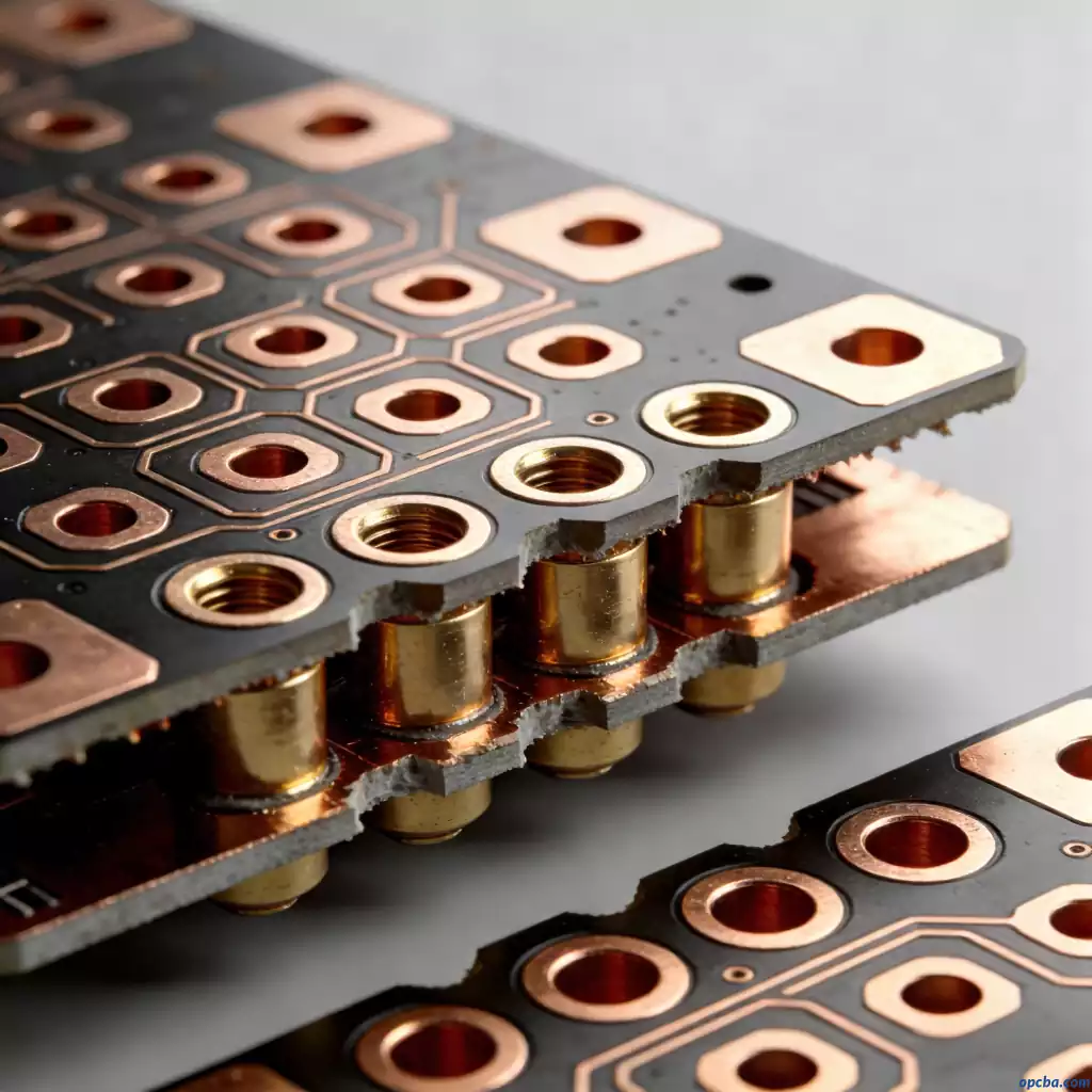
To begin with, PCB side plating—also commonly referred to as edge plating—is a specialized PCB fabrication technique involving copper plating that extends from the top surface to the bottom surface of a Printed Circuit Board(PCB), covering at least one of its perimeter edges. This process forms a continuous conductive pathway along the board’s edge, delivering a sturdy connection that minimizes the risk of device malfunctions—an essential feature for small PCBs, motherboards, and compact electronic modules like Wi-Fi and Bluetooth components. In terms of production, the edges targeted for metalization are first milled prior to copper plating, and appropriate surface treatment is applied afterward to ensure long-term durability and optimal performance.
1. When to Use PCB Side Plating?
Furthermore, PCB side plating is employed in specific scenarios where edge conductivity, structural integrity, or signal performance is critical:
- Improve PCB conductivity:Creates a low-resistance path for high-current applications, a key consideration in thermally demanding designs like Aluminum PCBs.
- Edge connections: Enables electrical connections directly at the board’s edge, such as in edge connectors.
- Lateral impact protection: Reinforces the board’s edges to resist physical damage from lateral impacts.
- Secondary PCB integration: Allows secondary boards to connect to motherboards via edge-mounted contacts.
- Edge soldering: Facilitates reliable soldering at the board’s edge to simplify assembly processes.
2. Types of PCB Side Plating
In addition, there are four primary types of PCB side plating, each tailored to specific design and manufacturing needs:
(1) Wrap-Around Edge Plating
Notably, wrap-around edge plating routes metal along the PCB’s sidewalls after drilling. The routing process exposes the PCB’s sidewalls to chemically plated base copper, which is applied simultaneously with the hole plating process. This creates a seamless conductive wrap around the board’s edge, ideal for applications requiring continuous edge conductivity.
(2) Copper Board Edge
Moreover, copper board edge plating requires specific minimum distances between copper features and the PCB edge to avoid damage:
- 0.25 mm on outer layers with breakout
- 0.40 mm on inner layers with breakout
- 0.45 mm on all layers with V-cut indentations
This type is suitable for flat surfaces and large copper areas where minor copper damage will not impact board performance. Tracks should not be placed within this minimum distance to prevent damage during manufacturing.
(3) Board Edge PTH
Additionally, board edge PTH (plated through holes) are cut at the PCB’s edge to enable joining two boards via direct soldering or connectors. During production, the PCB edge must have sufficient free space to hold the board in the production panel, and top/bottom layers require pads to secure the plating firmly in place.
(4) Rounded Edge Plating
Finally, rounded edge plating involves plating most or part of the PCB (or cutout) from top to bottom, primarily to establish a reliable ground connection for metal enclosures or shielding. To produce this type of board, the profile is milled before through-hole plating. Since 100% edge plating is not feasible (due to production panel constraints), routing tabs are used to secure the board during processing. Electroless nickel gold is the ideal surface finish for rounded edge plating.
Key Benefits of PCB Edge Plating
Furthermore, PCB edge plating delivers significant performance advantages:
- Enhances current conduction for high-power applications
- Ensures signal integrity by reducing electromagnetic interference (EMI)
- Improves electromagnetic compatibility (EMC) with surrounding systems
- Prevents electrostatic discharge (ESD) damage by providing a grounded edge
For professional guidance on PCB side plating and custom fabrication solutions, contact our experts at opcba.com to learn more.


