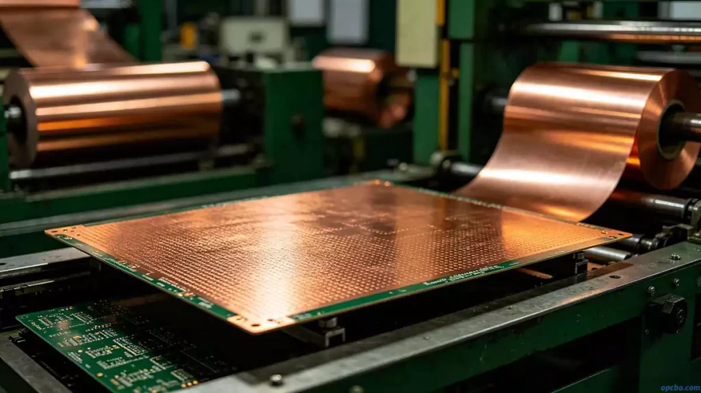
In our PCB factory, heavy copper PCB is becoming increasingly popular—especially for high-power devices. It’s a specialized PCB, defined by a copper thickness of 2oz or more.
Many clients we work with first ask: What is an “oz” in PCB terms? Let’s break that down simply, no jargon required.
In the PCB industry, “ounce (oz)” measures copper thickness. 1oz translates to roughly 36um of copper foil—derived from laying 1oz of pure copper (density 8.9g/cm³) flat over 1 square foot (144 square inches).
Standard PCBs use 0.5oz or 1oz copper foil. Once the inner and outer copper thickness hits 2oz or more, it’s classified as a heavy copper PCB.
Heavy Copper PCB vs. Regular Copper PCB: Key Advantages
Copper foil acts as the board’s conductor, working to maximize electrical performance. But conducting electricity generates heat—and copper thickness directly impacts heat dissipation.
Heavy copper PCBs outperform regular ones here: they carry more current, reduce thermal strain, and offer better heat dissipation. We’ve seen this firsthand in high-power projects.
1. Higher Current-Carrying Capacity
With a fixed line width, increasing copper thickness boosts the circuit’s cross-sectional area. That means it can handle more current—critical for high-power devices.
2. Reduced Thermal Strain
Copper has low resistivity (excellent conductivity, second only to silver). Under high current, it heats up less—cutting down on thermal strain.
Thermal strain refers to geometric/ dimensional changes when materials heat up or cool down. In practice, this strain can warp thin copper PCBs over time—something we avoid with heavy copper.
3. Superior Heat Dissipation
Copper’s thermal conductivity is 401W/mK—impressive for heat transfer. This keeps boards cool, lowering the risk of burnout.
It’s why heavy copper PCB is our go-to for high-current designs. We’ve used them in power supplies where overheating was a frequent issue with regular PCBs.
Beyond these, heavy copper PCBs have thickened copper in PTH (plated through holes) and sidewalls. This strengthens component connections, improves synergy between components and the board, and even reduces end-product size.
Key Considerations for Heavy Copper PCB Manufacturing
Standard PCB substrates use 0.5oz or 1oz copper. To reach 2oz+, we rely on electroplating to thicken the base copper—this process is called copper plating.
After plating, we etch the PCB to achieve the customer’s designed electrical performance. But thick copper etching comes with challenges.
For a full breakdown of etching technology and requirements for high-quality PCBs, explore our guide: PCB Etching Technology and Basic Requirements.
When etching thick copper lines, the etchant eats away at the line sides (side etching) while removing excess copper. Thicker copper means longer etching times, worse side etching, and a higher chance of trapezoidal lines.
To prevent lines from thinning, our production team pre-compensates based on the finished copper thickness. This is why hardware engineers must widen line spacing in design—too little spacing leads to thin lines or open circuits during exposure and etching.
Special Processes for Heavy Copper PCB Production
From our factory experience, these are the critical steps for heavy copper PCB manufacturing process:
- Electroplating: Both inner and outer layers need electroplating to thicken base copper to 2oz+. For high-integration boards (aspect ratio ≥10:1), immersion copper plating gets tricky.
- Etching: Inner and outer line etching is more difficult than with regular PCBs, requiring precise parameter control.
- Inner layer resin filling: Necessary before press-fit to ensure board flatness.
- Multiple soldermask prints: Thick copper requires extra soldermask layers for proper coverage.
Where Heavy Copper PCBs Are Used
Thanks to their high current-carrying capacity and excellent heat dissipation, heavy copper PCBs are a top choice for high-power device manufacturers.
We supply them to clients in power supplies, solar panel equipment, medical devices, automotive, aviation, and welding equipment—all fields where reliability under high current matters most.


