In the complex structure of a PCB, copper foil serves as the core conductive component, and the choice of its thickness has a decisive impact on PCB performance. PCB copper thickness is not fixed—engineers select from a wide range of specifications based on different application scenarios and performance requirements. We typically measure standard PCB copper thickness in ounces per square foot. This value represents the weight of copper per square foot of area. It can be converted to thickness in micrometers or mils (1 mil = 0.001 inch). Standard PCB copper thickness varies depending on the specific application and performance requirements of the PCB.
Standard Copper Thicknesses in PCB Design
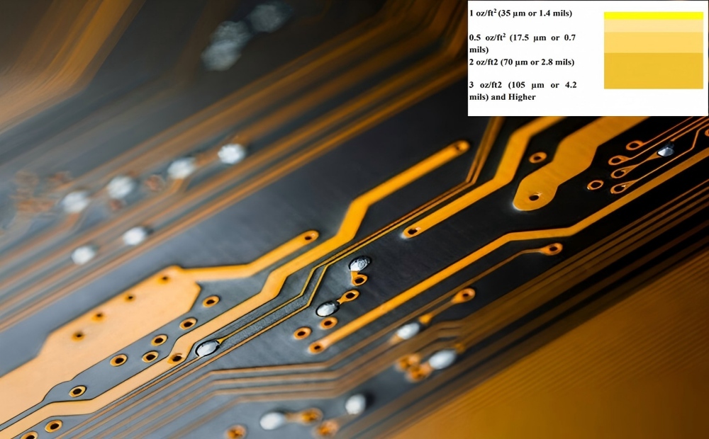
- 1 oz/ft² (35 microns or 1.4 mils): This is the standard copper thickness for most PCBs on the market. This standard PCB copper thickness is more suitable for general-purpose circuit boards with moderate current requirements and typical board sizes.
- 0.5 oz/ft² (17.5 microns or 0.7 mils): This thinner copper layer works in space-constrained applications. We also use it for low-power circuit boards. This design is common in small devices, and engineers typically use it for fine-pitch designs.
- 2 oz/ft² (70 µm or 2.8 mils): This represents a thicker copper layer, primarily used in high-current applications where the PCB needs to handle higher currents without generating excessive heat.
- 3 oz/ft² (105 µm or 4.2 mils) and above: We use these heavy copper PCB thicknesses in specialized high-power applications, such as power supply boards and automotive electronics. This thickness meets the demand for high current-carrying capacity without significant overheating.
In most cases, the standard copper thickness for general-purpose PCB designs is 1 oz/ft² (2 oz/ft²). This achieves a good balance between electrical performance and PCB manufacturing.
Copper Thickness Characteristics for Flexible Printed Circuits
For flexible printed circuits (FPCs), copper thicknesses also have specific ranges, with common options including 9 μm, 12 μm, and 18 μm. Due to their bendable and foldable properties, flexible printed circuits are widely used in applications such as wearable devices and internal wiring in mobile phones.
- 9μm and 12μm Copper Foil: A Lightweight and Comfortable Choice: Taking the FPC in a smart wristband as an example, a copper foil thickness of 9μm or 12μm meets the requirements for lightness and flexibility, allowing the wristband to fit comfortably on the wrist while also enabling signal transmission and basic circuit functions.
- 18μm Copper Foil: Balancing Strength and Performance: 18μm copper foil is used in applications with slightly higher requirements for the strength and electrical performance of flexible circuit boards. For example, in some high-end smartphones, the flexible cables connecting the display to the motherboard must maintain a stable electrical connection through repeated bending. The relatively superior toughness and electrical performance of 18μm copper foil meet this demand.
Copper Thickness for Special Applications
In certain specialized applications, even thicker or thinner copper foils may be required.
- Extra-Thick Copper Foil—A Powerhouse for High-Power Applications: For example, in thick-copper PCBs using FR-4 as the base material, special processes can increase the copper foil thickness to 2 ounces (70 μm) or more, reaching levels of 4 ounces (140 μm), 5 ounces (175 μm), or even higher. This ultra-thick copper foil excels in applications requiring efficient current transmission and robust heat dissipation, such as high-power electronic devices, power conversion systems, and planar transformers.
- Ultra-thin Copper Foil—The Pioneer of High-Frequency and High-Speed Applications: Conversely, as electronic technology continues to evolve toward miniaturization and higher performance, the challenge of pushing the lower limit of PCB copper thickness persists. Currently, some advanced manufacturing processes are capable of producing 3.5-micron copper foil. This ultra-thin copper foil can be applied in fields with extremely high requirements for signal transmission speed and loss, such as 5G, 6G, and even future AI servers, enabling faster signal transmission with lower loss.
Three Key Factors Influencing PCB Copper Thickness Selection
The selection of copper thickness is not simply a matter of “thicker is better,” but rather requires a comprehensive consideration of current-carrying capacity, heat dissipation requirements, and signal characteristics. Different factors result in significantly varying requirements for copper thickness.
Current-Carrying Capacity: Thickness Determines the Upper Limit of Current Flow
The current-carrying capacity of copper foil is directly proportional to its thickness. The thicker the copper foil, the greater the current it can carry. According to Jiepei’s insights, for every 1 oz increase in thickness, current-carrying capacity increases by approximately 50% to 80%. Industry-standard current-carrying guidelines (25°C ambient temperature, continuous operation) also provide detailed references. For example, 0.5 oz copper foil with a width of 1 mm can carry 0.5 to 0.8 A; 1 oz copper foil with a width of 1 mm can carry 1.0 to 1.5 A; and 2 oz copper foil, 1 mm wide, can handle 1.8–2.5 A.
Heat Dissipation Efficiency: Thicker Copper Foil Enhances Thermal Conductivity
Copper has a thermal conductivity of approximately 401 W/(m·K), far exceeding that of the FR-4 substrate (0.3–0.5 W/(m·K)). Therefore, copper foil thickness directly impacts the PCB’s thermal conductivity. We apply thin copper foil to low-power applications—like mobile phone CPUs—where convection on the PCB surface provides primary heat dissipation. For medium-to-high-power applications, such as automotive MCUs, we use thick copper foil to conduct heat to a heat sink. For high-power scenarios like new energy inverters, we rely on ultra-thick copper foil, which requires heat-dissipating vias and a metal enclosure.
Signal Integrity: Thin Copper Foil Suits High-Frequency Signals
When high-frequency signals propagate through copper foil, the “skin effect” occurs, causing current to concentrate on the foil’s surface, which leads to signal loss. Therefore, we tailor PCB copper thickness to match signal frequency characteristics. For high-frequency signals (> 1 GHz), we typically select thin copper foil of 1 oz or less; overly thick foil increases surface roughness, which will cause severe signal attenuation. For low-speed signals (< 100 MHz), copper thickness is less critical, and we recommend choosing 1–2 oz copper foil based on actual current demands to ensure stable signal transmission and reduce unnecessary energy loss.
Correlation Between Copper Foil Type and Thickness
Different types of copper foil (electrolytic copper foil and rolled copper foil) have distinct thicknesses and applications. Electrolytic copper foil ranges from 0.5 to 5 oz in thickness, has higher surface roughness, is lower in cost, and is suitable for general-purpose current conduction and heat dissipation applications. Rolled copper foil has a thickness range of 0.3–2 oz, low surface roughness, and good ductility, making it suitable for high-frequency signals and flexible PCBs.
Applications and Use Cases for Different Copper Thicknesses
The selection of standard PCB copper thickness depends on the specific requirements of the application. The following lists some use cases for different standard PCB copper thicknesses.
- 0.5 oz/ft² copper: We typically use this standard PCB copper thickness for low-power circuits, fine-pitch designs, and space-constrained devices. It serves mainly in mobile devices, wearable electronics, and other compact, lightweight products that demand only low current. This specific standard PCB copper thickness helps save significant space, enables finer trace routing, and facilitates the construction of miniature designs.
- 1 oz/ft² copper: This is the thickness grade we use in general PCB manufacturing. It is the most common standard PCB copper thickness on the market. We typically use it in consumer electronics, telecommunications equipment, and computers. This standard PCB copper thickness strikes a good balance between current-carrying capacity and manufacturability, making it the most widely used standard.
- 2 oz/ft² copper: We primarily use this standard PCB copper thickness for high-current applications and power circuits. They are also suitable for power supplies, automotive electronics in industrial control systems, and motor drivers. These standard copper thicknesses support higher currents and have low heat dissipation, making them ideal for high-end equipment.
- 3 oz/ft² Copper: This standard PCB copper thickness is particularly suitable for high-power applications, such as heavy-duty power electronics, electric vehicles, industrial power distribution, and renewable energy systems. The advantage of PCBs with this standard copper thickness lies in their ability to handle extremely high currents while providing excellent heat dissipation. The drawback of this thickness is higher manufacturing costs and greater complexity.
Summary
With the rapid development of emerging industries such as 5G and new energy vehicles, higher demands are being placed on PCB design. A thorough understanding and precise selection of PCB copper thickness is key to ensuring product performance and reliability. How do you think High-Density Interconnect (HDI) technology and more advanced PCB materials will influence the selection and application of copper foil in the future?


