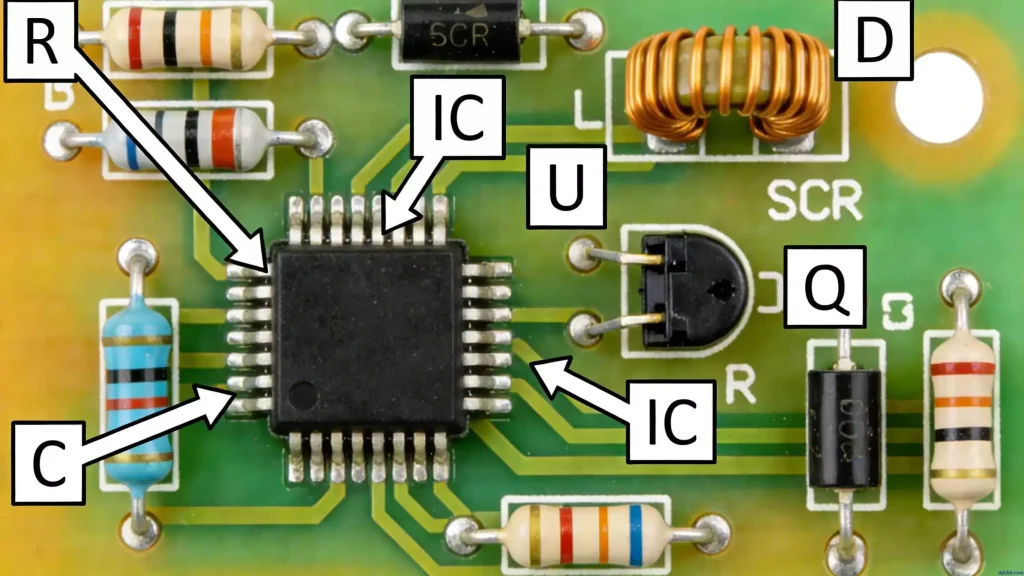
If you’ve ever held a modern smartphone, worn a smartwatch, or used a laptop, you’ve held the result of surface mount technology. It’s the manufacturing method behind virtually every compact electronic device in existence today. But for PCB designers and engineers, understanding surface mount technology isn’t just about knowing what it is—it’s about knowing how to design for it. If you’re new to core printed circuit board fundamentals and terminology, start with our foundational overview: Printed Circuit Board(PCB)
This guide covers the full picture: what SMT is, how the assembly process works, and—most importantly—what PCB design decisions directly impact SMT yield and reliability.
1. What Is Surface Mount Technology?
Surface mount technology (SMT) is a method of constructing electronic circuits in which components are mounted directly onto the surface of printed circuit boards (PCBs). The components used in this process are called surface-mount devices (SMDs).
Surface mount technology began to emerge during the 1960s through innovations by IBM and other electronics manufacturers. Commercial adoption accelerated rapidly throughout the 1980s. By the early 1990s, SMT had become the dominant assembly technology for most consumer and industrial electronics.
The key distinction: In traditional through-hole technology (THT), component leads pass through drilled holes in the PCB and are soldered on the opposite side. In SMT, components are soldered directly onto flat copper pads on the board’s surface. This seemingly simple difference has profound implications for size, cost, and performance.
For designers working with surface mount technology, IPC standards provide the foundation for reliable land pattern design. While IPC-7351 provides the general framework for SMT land pattern design, the component manufacturer’s recommended footprint should always take precedence whenever available. Additional IPC standards relevant to SMT assembly include IPC-A-610 (Acceptability of Electronic Assemblies) and IPC-7095 (Design and Assembly Process Implementation for BGAs).
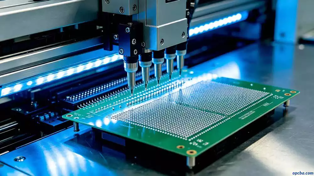
2. The SMT Assembly Process Step by Step
A modern SMT assembly line is a marvel of high-speed automation. The process consists of four critical phases. Understanding each phase helps PCB designers make better layout decisions.
Phase 1: Solder Paste Printing
The process begins with solder paste printing. A precision metal stencil is aligned over the bare PCB, and a squeegee blade deposits a precise volume of solder paste onto the surface pads.
What PCB designers need to know: The stencil aperture design is directly linked to your pad design. For fine-pitch components (e.g., 0.4mm pitch BGAs), the aspect ratio and area ratio of the stencil openings must be carefully calculated to ensure proper “paste release.” If your pads are too small or too closely spaced, the stencil won’t print reliably.
Solder paste itself is a thixotropic mixture of microscopic solder spheres in a flux medium. For modern lead-free processes, SAC305 (96.5% tin, 3% silver, 0.5% copper) is the industry standard, paired with a “no-clean” flux that doesn’t require post-assembly washing.
Phase 2: Automated Pick-and-Place
High-speed robotic heads fitted with optical alignment cameras and vacuum nozzles pull SMDs from component reels and place them onto the sticky solder paste. Modern high-speed placement systems can exceed 100,000 components per hour (CPH), depending on machine configuration and component mix, handling packages as small as 0201 and even 01005 (Imperial) based on machine capability.
What PCB designers need to know: Component orientation matters. Consistent component orientation simplifies programming, automated inspection, and manual rework while reducing setup complexity. Fiducial markers—small copper pads used by the machine’s vision system for alignment—must be placed correctly. Missing or improperly positioned fiducials may reduce placement accuracy, increase setup time, or require additional manual alignment.
Phase 3: Reflow Soldering
The populated board travels on a conveyor belt through a multi-zone reflow oven. The oven ramps up the temperature to activate the flux, liquefies the solder alloy (typically reaching peak temperatures of 235–250°C depending on the solder alloy, PCB design, and component specifications), and then cools to form durable metallurgical joints.
What PCB designers need to know: Thermal mass differences between components can cause uneven heating. Large components (connectors, BGAs) take longer to heat up than small passives (resistors, capacitors). This can lead to cold solder joints on large components or overheating on small ones. Designers should consider component placement distribution to promote even heating.
Phase 4: Automated Inspection
The completed assembly passes through automated optical inspection (AOI) systems. High-resolution cameras and multi-angled lighting check for component misalignments, tombstoning, or solder bridges. For hidden connections like BGAs, 3D X-ray systems are used to verify internal joint structure.
What PCB designers need to know: Inspection is only as good as the board’s design. Extremely small features, insufficient component spacing, reflective surfaces, or excessive shadowing may reduce AOI inspection accuracy. Design for inspectability (DFI) is just as important as design for manufacturability.
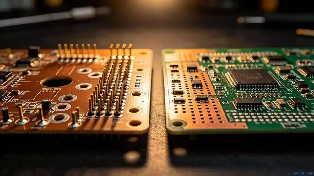
3. PCB Design Rules for SMT Success
This is where most guides stop—but for PCB designers, this is where the real work begins. Here are the specific layout rules that directly impact SMT yield. Unless otherwise specified, footprint recommendations should follow IPC-7351 or the component manufacturer’s datasheet. According to IPC-7351, land pattern dimensions should be derived from the component’s physical dimensions, with adjustments for solder joint formation and inspection requirements.
Pad Design
Pad dimensions must match the component’s footprint precisely. Too small, and the component won’t solder properly; too large, and the component may shift during reflow.
| Component Type | Typical Reference Pad Dimensions (Reference Only) | Notes |
|---|---|---|
| 0201 passives | 0.3 × 0.4mm | Requires high-precision printing |
| 0402 passives | 0.5 × 0.6mm | Most common, well-established |
| 0603 passives | 0.8 × 0.9mm | More forgiving, good for prototypes |
| QFP (0.5mm pitch) | Pad width = 0.25–0.30mm | Follow IPC-7351 for exact dimensions |
| BGA (0.8mm pitch) | Pad diameter = 0.40–0.45mm | Follow manufacturer’s land pattern |
Note: Actual land patterns should always follow IPC-7351 or the component manufacturer’s recommended footprint. For BGAs, always follow the package manufacturer’s recommended land pattern.
Solder Mask Design
Solder mask is the green (or other color) coating that covers the copper traces, leaving only the pads exposed.
- For most fine-pitch ICs, including QFPs, QFNs, and BGAs, Non-Solder Mask Defined (NSMD) pads are generally preferred because, according to IPC-7351, they provide better solder joint reliability and more consistent solder wetting.
- Solder Mask Defined (SMD) pads may be used in certain HDI designs where solder mask webbing becomes too narrow to manufacture reliably.
- Solder mask bridge (web) width: The minimum solder mask bridge should follow your PCB manufacturer’s fabrication capability, typically around 0.08–0.10mm for fine-pitch components. For a full systematic guide covering solder mask types, production processes, and complete design specifications, check our dedicated article: Soldermask in PCB production
Fiducial Marks
Fiducial marks are small copper pads (typically 1mm diameter) that the pick-and-place machine uses to align the board.
- Place at least three fiducial marks on the board—one in each corner, with one offset to define orientation.
- Fiducials should be clear of solder mask (copper exposed) and placed on a background with high contrast.
- Do not place fiducials too close to the board edge—keep at least 3mm clearance.
Component Spacing
Components need adequate spacing for placement, soldering, and inspection. According to IPC-7351 recommendations, the following minimum spacings are typical:
| Component Type | Minimum Spacing |
|---|---|
| Small passives (0201–0603) | 0.3mm between components |
| Larger passives (0805+) | 0.5mm between components |
| ICs (QFP, QFN) | 0.5mm from other components |
| BGAs | 1.0mm from other components |
Component Orientation
For components with polarity or pin 1 marking, all components should be oriented in the same direction where possible. Consistent component orientation simplifies programming, automated inspection, and manual rework while reducing setup complexity.

4. SMT vs Through-Hole: When to Use Which
Surface mount technology is the dominant assembly technology used in the vast majority of modern electronic products, but through-hole technology hasn’t disappeared—and it won’t. Here’s how to decide.
Quantitative Comparison
| Metric | SMT | Through-Hole |
|---|---|---|
| Component size | Much smaller | Larger |
| PCB size | Significantly reduced | Baseline |
| Assembly speed | >100,000 parts/hour (high-end) | Manual or slower automated |
| Drilling required | No | Yes—time-consuming and expensive |
| Mechanical strength | Lower (solder joint only) | Higher (lead through hole) |
| High-frequency performance | Better (shorter leads, less parasitics) | Worse (leads act as antennas) |
| Rework difficulty | Difficult | Easier |
| Capital investment | High | Lower |
Decision Framework
Choose SMT when:
- You need high component density or compact size
- You’re producing high volumes (automation pays off)
- The circuit operates at high frequencies (>100MHz)
- You want to populate both sides of the board
Keep Through-Hole when:
- Components must withstand mechanical stress (connectors, large transformers)
- You’re prototyping or doing low-volume production
- The component is only available in through-hole package
- You need very high power handling
The hybrid approach: Many designs use SMT for most components and THT only for connectors, large capacitors, or components that experience mechanical stress. When mixing technologies, place THT components on the same side of the board to simplify the soldering process.
5. Common SMT Defects and How to Prevent Them at PCB Design Stage
Many SMT defects are blamed on the assembly line, but the root cause often lies in the PCB design. Here are the most common defects and what designers can do to prevent them.
Tombstoning (Component Lifting)
What it looks like: One end of a small passive component (resistor, capacitor) lifts off the pad during reflow, standing up like a tombstone.
Root cause: Uneven heating or uneven solder paste volume on the two pads. One end reflows before the other, and the surface tension pulls the component upright.
Design-side prevention:
- Ensure pad sizes are symmetrical for two-terminal components
- Avoid placing small components near large heat sinks that create thermal gradients
- Use thermal relief connections to balance heating on pads connected to large copper planes. Thermal reliefs are particularly important for pads connected to ground planes or power planes, as these large copper areas can sink heat away from the pad during soldering.
Solder Bridging
What it looks like: Solder connects two adjacent pads that should be isolated, creating a short circuit.
Root cause: Too much solder paste, pads too close together, or insufficient solder mask between pads.
Design-side prevention:
- Maintain adequate spacing between adjacent pads (see spacing table above)
- Use Non-Solder Mask Defined (NSMD) pads for most fine-pitch ICs
- Ensure the solder mask bridge between pads meets your manufacturer’s fabrication capability (typically 0.08–0.10mm)
Solder Balling and Voiding
What it looks like: Small solder balls scattered around the board, or voids (empty spaces) inside BGA solder joints.
Root cause: Oxidation on pads, incorrect reflow profile, or outgassing from trapped flux.
Design-side prevention:
- Ensure pads are clean and properly finished (ENIG or OSP are commonly used)
- For BGAs, avoid placing vias directly in the pad (via-in-pad) unless they’re filled and plated over—unfilled vias can wick solder away and create voids. IPC-7095 provides detailed guidance on BGA via design and voiding prevention.
- Use appropriate pad sizes for BGAs—always follow the package manufacturer’s recommended land pattern
Insufficient Wetting (Cold Joints)
What it looks like: Solder hasn’t fully melted or hasn’t wetted the component lead, resulting in a dull, grainy joint.
Root cause: Insufficient heat, contaminated pads, or incorrect solder paste.
Design-side prevention:
- Use appropriate surface finish for your assembly process. ENIG is one of the most commonly recommended finishes for fine-pitch SMT because of its flat surface and excellent solderability.
- Ensure pad designs match the component footprint exactly—following IPC-7351 recommendations
- For large components with high thermal mass, consider adding thermal vias to help heat reach the pads

6. SMT Design Checklist for PCB Layout Engineers
Use this checklist before finalizing your PCB layout:
- Component footprints verified against manufacturer datasheets or IPC-7351
- Non-Solder Mask Defined (NSMD) vs Solder Mask Defined (SMD) pads selected appropriately
- Solder mask bridge width meets manufacturer capability (typically 0.08–0.10mm for fine-pitch)
- Pad sizes: symmetrical for two-terminal components
- Component spacing meets IPC-7351 recommendations:
- 0201–0603: ≥0.3mm between components
- 0805+: ≥0.5mm
- ICs: ≥0.5mm from other components
- BGAs: ≥1.0mm from other components
- Fiducial marks: at least 3 placed, 1mm diameter, solder mask clear
- Component orientation: pin 1/polarity aligned in same direction where possible
- Thermal relief used on pads connected to large copper pours or power/ground planes
- No unfilled vias in BGA pads (unless filled and plated)
- Surface finish selected according to product requirements (ENIG, OSP, Immersion Silver, etc.)
- Panelization and break-away tabs considered if board is small
- DFM and DFI (Design for Inspectability) review requested from assembly house
Conclusion: Design for SMT from Day One
Surface mount technology is the backbone of modern electronics manufacturing. But the difference between a board that assembles smoothly and one that suffers from low yield, rework, and delay often comes down to PCB design decisions made weeks before the board ever reaches the assembly line.
For PCB designers and engineers, the key takeaway is this: SMT isn’t just an assembly process—it’s a design constraint. Pad sizes, component spacing, fiducial placement, solder mask design, and thermal management all influence whether your board can be assembled reliably and cost-effectively.
Following industry standards such as IPC-7351 for land pattern design, IPC-A-610 for assembly acceptability, and IPC-7095 for BGA implementation ensures your design meets the expectations of most contract manufacturers and assembly houses.
If you’re developing a PCB and need engineering review for SMT assembly, send your design files to OPCBA. Our engineering team provides DFM review for SMT assembly, footprint verification, and assembly process recommendations—typically within one business day of receiving your Gerber files. For inquiries or to submit your design for a free manufacturability check, email us directly at sales@opcba.com.