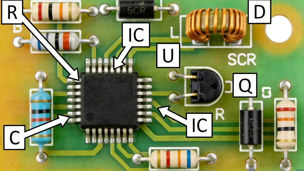
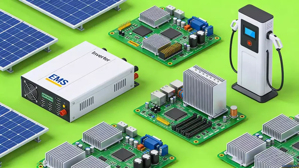
Integrated circuit (IC) packaging is a critical process that connects semiconductor chips with external electronic systems. Specifically, after fabricating and testing wafers, manufacturers package and test bare dies prior to PCB assembly.
The main purpose of IC packaging is to protect the semiconductor die, provide electrical connections, improve heat dissipation, and enable reliable mounting on a PCB.
Different IC package types have different structures, sizes, pin configurations, and electrical characteristics. As a result, these differences directly affect PCB design requirements.
What Is IC Packaging?
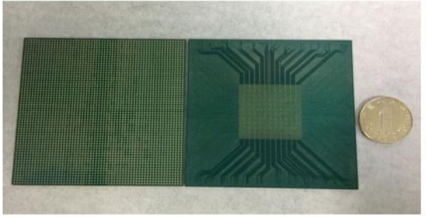
IC packaging is the process of connecting a semiconductor die with external electrical terminals and protecting it with a suitable package structure.
In packaging, manufacturers mount bare silicon dies on substrates or lead frames, establish connections through wire bonding or advanced interconnection technologies, and encapsulate them with plastic, ceramic, or other packaging materials.
The completed package is IC package or semiconductor package.
The package provides several important functions:
- Protects the semiconductor die from physical damage and contamination
- Provides electrical connections between the chip and PCB
- Improves heat dissipation performance
- Enables efficient PCB assembly and soldering
Types of IC Packages
1. IC Package Types by Packaging Material
According to the packaging material, IC packages mainly include:
Metal Packages
Metal packages provide excellent mechanical strength and thermal performance.
Due to their relatively high cost, they occupy only a small portion of commercial applications.
Ceramic Packages
Ceramic packages offer excellent thermal stability, reliability, and environmental resistance.
They are commonly in specialized applications requiring high reliability, including aerospace and industrial electronics.
Plastic Packages
Plastic packages are the most widely used package type in consumer electronics.
Advantages include:
- Low manufacturing cost
- Simple production process
- Good reliability
- Suitable for mass production
Most modern electronic products use plastic IC packages because of their cost-effectiveness.
2. IC Package Types by Connection Method
According to the connection method between the IC package and PCB, packages can be divided into:
Through-Hole Package (PTH)
Through-hole packages use leads that pass through holes drilled in the PCB and are soldered on the opposite side.
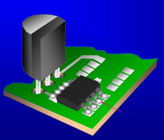
A typical example is DIP (Dual In-line Package).
Advantages:
- Strong mechanical connection
- Suitable for high-reliability applications
- Easy for manual soldering and replacement
However, through-hole packages require more PCB space and are less suitable for high-density electronic products.
Surface Mount Package (SMT)
Surface mount packages are directly soldered onto PCB surface pads without requiring drilled holes.
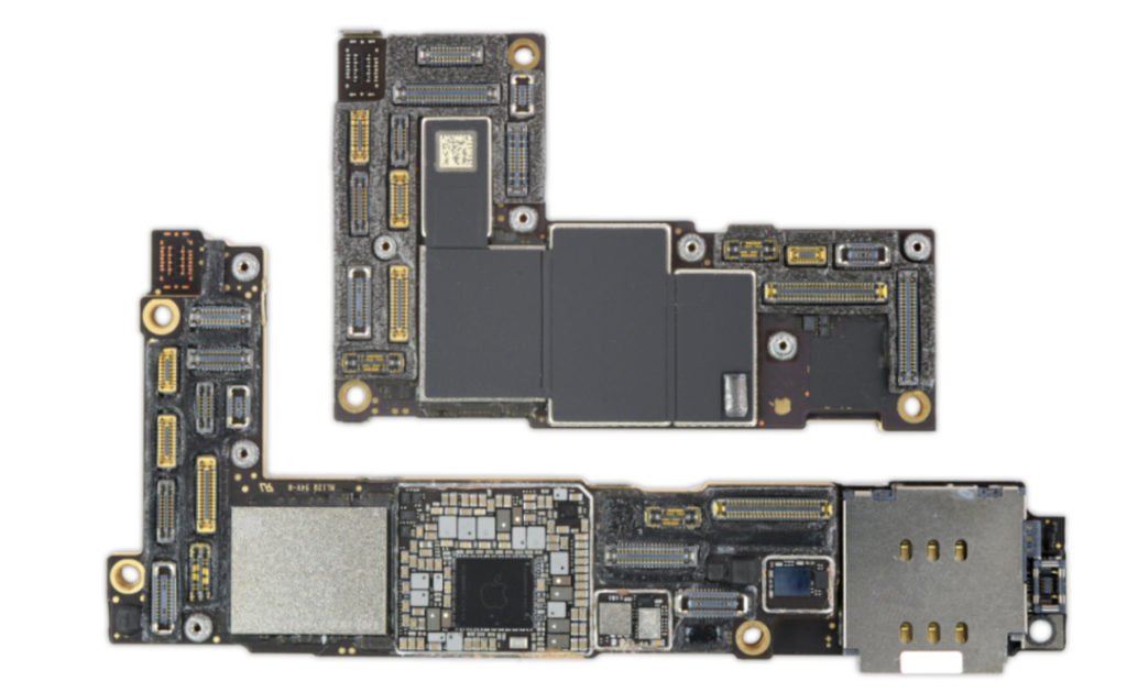
Common SMT packages include:
- SOIC
- TSSOP
- QFN
- QFP
- BGA
- CSP
3. Common IC Package Structures
Different applications require different IC package structures.
Common package types include:
QFP (Quad Flat Package)
QFP packages use leads extending from four sides of the package.
Advantages:
- Easy visual inspection
- Mature manufacturing process
They are commonly used in microcontrollers and industrial electronic products.
BGA (Ball Grid Array)
BGA packages use solder balls arranged in a grid pattern underneath the package.
Compared with traditional lead packages, BGA provides:
- Higher I/O density
- Better electrical performance
- Improved thermal performance
However, BGA packages require advanced PCB manufacturing capabilities, including:
- Fine-pitch PCB fabrication
- HDI technology
- Microvia processing
- Precise impedance control
BGA is widely used in processors, communication devices, and high-performance electronic products.
CSP (Chip Scale Package)
CSP is a compact package technology where the package size is close to the size of the semiconductor die.
It is commonly used in mobile devices, memory chips, and miniaturized electronic products.
In the next article, in detail, we will further introduce the semiconductor packaging process, including wafer inspection, wafer thinning, dicing, die attach, wire bonding, molding, and final testing, to help you better understand how a semiconductor die becomes a complete IC package ready for PCB assembly.