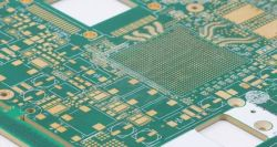
RF PCBs (Radio Frequency Printed Circuit Boards) are specifically designed to handle RF signals efficiently. If your circuit board operates at frequencies above 100 MHz, it qualifies as an RF PCB. These boards ensure the proper functioning of high-frequency circuits during the transmission or reception of radio signals and are vital to today’s wireless communication landscape.
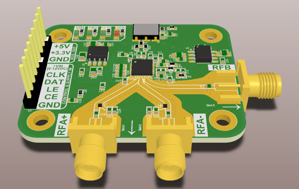
Types of RF PCB
Rigid RF PCBs
Rigid RF PCBs are manufactured using materials suitable for high-speed RF operations. They can be designed as single-layer, double-layer, or multi-layer boards. Most designs utilize a multi-layer structure because embedded impedance control is crucial for accurate signal transmission. In a multi-layer stack-up, copper traces and dielectric substrates are meticulously layered; this structure helps reduce noise and maintain signal integrity, even at high frequencies.
Flexible RF PCBs
Flexible RF PCBs are made from bendable materials, such as polyimide or polyester. They are essential when a design requires folding or installation within tight, irregular spaces. Offering excellent flexibility reduces the risk of breakage, they are ideal for compact devices that have limited space and require frequent movement.
Rigid-Flex RF PCBs
Rigid-flex RF PCBs combine rigid and flexible sections into a single, continuous circuit board, offering the mechanical strength of a rigid substrate alongside the adaptability of a flexible circuit. While this combination increases design complexity, it maintains excellent electrical stability, thereby enhancing RF performance. Each section must be precisely engineered to ensure consistent signal transmission across the entire structure.
High-Frequency RF PCBs
These boards are specifically designed for signal operation within the gigahertz range. At such high frequencies, material selection is critical; substrates must feature a low dielectric constant and minimal dissipation factor (loss tangent). These properties help prevent signal attenuation and maintain transmission clarity. Even minor deviations can lead to significant performance loss, making precision in materials and layout essential.
RF Antenna PCBs
RF antenna PCBs are designed for circuits that incorporate or integrate an antenna. In some designs, the PCB itself functions as the antenna element. The layout focuses on achieving appropriate gain, impedance matching, and a stable radiation pattern. Such circuit boards are commonly found in wireless communication modules, IoT devices, and RFID systems, where compact and efficient antenna integration is crucial.
How does RF PCB design differ from standard PCB design?
In low-frequency or digital PCBs, traces primarily serve as simple interconnects; if components are connected correctly, the circuit usually functions properly. RF PCBs, however, operate quite differently.
At high frequencies:
- Signals behave like waves rather than just electric current.
- Trace width and spacing affect impedance, not merely resistance.
- Signal integrity becomes critical, along with risks such as reflections and signal loss.
- Layout directly impacts performance; even minute changes can lead to instability.
Therefore, RF PCB design requires controlled-impedance routing, reliable grounding, and a carefully engineered layout. Material selection and stack-up structure also play a more significant role than in standard PCB design.
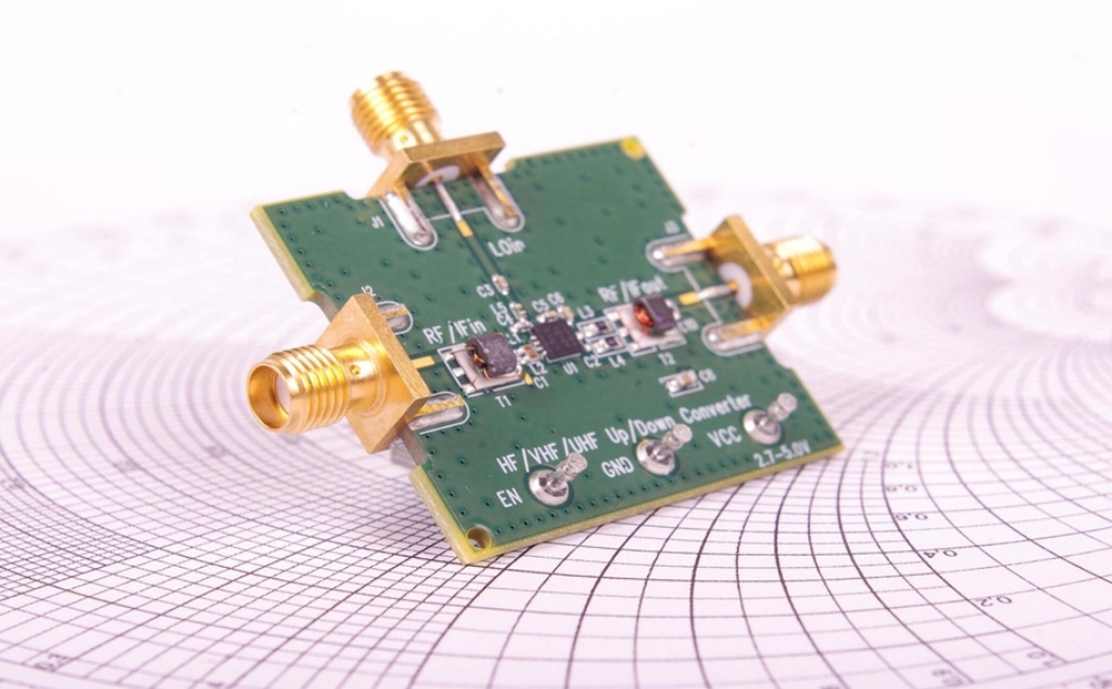
Key concepts in RF PCB design
RF PCB design focuses primarily on how high-frequency signals propagate across the circuit board. At these frequencies, signals do not travel merely as simple current paths but rather behave like waves, making board layout and material selection critical.
RF signal behavior and frequency effects
As frequency increases, signals become more sensitive to trace length, routing geometry, and surrounding structures. Even slight layout variations can affect signal timing and strength. Vias, sharp corners, or abrupt changes in trace width can disrupt signals and degrade performance. Consequently, RF PCB layouts must be kept clean, compact, and consistent.
Impedance and controlled-impedance traces
In RF PCBs, traces are designed to maintain a specific impedance—typically 50 ohms. This facilitates smooth signal transmission from the source to the load.
If trace impedance fluctuates, a portion of the signal reflects back, weakening the signal and causing distortion. Controlled impedance depends on trace width, spacing, and the PCB stack-up structure.
Signal Integrity, Electromagnetic Interference (EMI), and Loss
High-frequency signals are more prone to energy loss and can interfere with other circuits. Losses can stem from PCB materials, copper resistance, or radiation.
Additionally, if RF signals are not properly controlled, electromagnetic interference may occur. Effective RF PCB design employs reliable ground planes, smooth routing, and appropriate spacing to maintain signal stability.
RF PCB Material Selection
Material selection is critical in RF PCB design. At high frequencies, PCB materials influence signal propagation speed, signal loss, and long-term circuit stability.
Dk, Df, and Material Stability
The dielectric constant (Dk) affects signal speed and impedance. Changes in Dk result in corresponding changes to signal characteristics. The dissipation factor (Df) indicates the amount of signal energy lost as heat; a lower Df means less loss and superior RF performance. Material stability is crucial because RF PCBs often operate in environments with fluctuating temperatures. Stable materials help ensure consistent signal performance.
High-Frequency PCB Materials
RF PCBs typically utilize specialized materials designed for high-frequency signals. PTFE-based and ceramic-filled laminates are common choices due to their low loss and stable electrical performance. These materials are widely used in RF and microwave circuits.
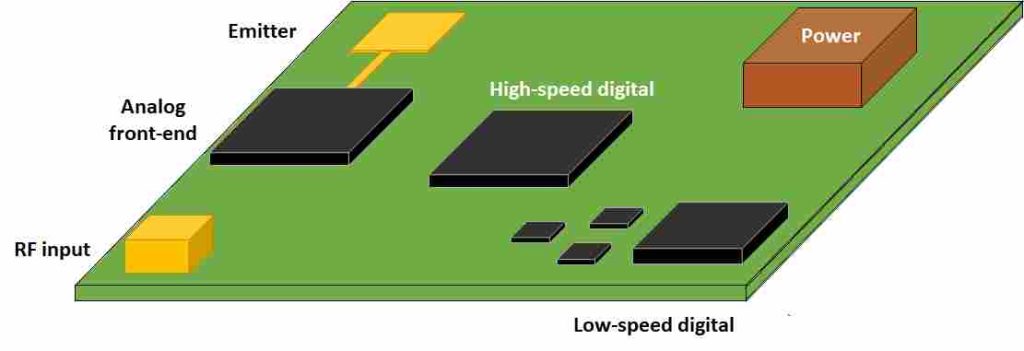
Comparison: FR-4 vs. RF Materials
While FR-4 is a common and cost-effective material, its high loss at high frequencies limits RF performance. RF materials are more expensive but offer lower loss and greater impedance stability.
FR-4 may be suitable for low-frequency designs, whereas RF materials are better suited for high-frequency applications.
Summary
As core components of modern electronic devices, the design, manufacturing, and application of RF PCBs demonstrate a high level of professionalism and technical sophistication. With technological advancements and growing market demand, this field will continue to maintain its vitality for innovative development.