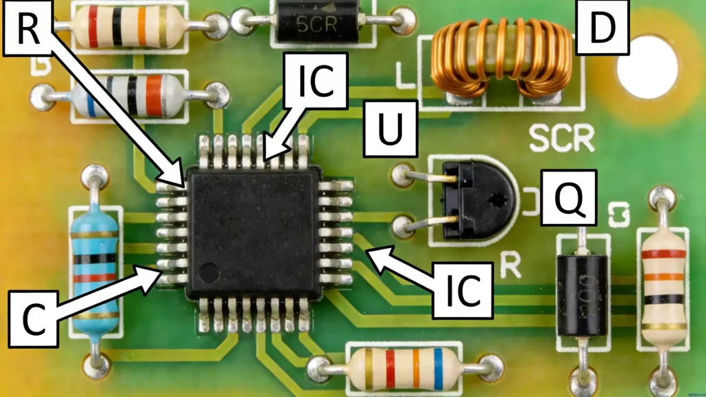
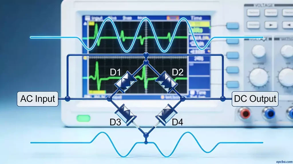
A PCB (Printed Circuit Board) provides the electrical connections for electronic components. The layout of components in PCB design is crucial, affecting the final performance of the product.
An unreasonable component layout and arrangement will lead to a decline in the electrical and mechanical performance of the product. It will also cause inconvenience in assembly and maintenance. So how should PCB components be laid out reasonably?
PCBA Control Board Component Layout Considerations
1. In the PCB layout design, related components should as close as possible. For example, clock generators, crystal oscillators, and CPU clock input terminals are prone to noise. They should close to each other.
For devices that are prone to noise, low-current circuits, high-current switching circuits, etc., they should as far away as possible from microcontroller logic control circuits and memory circuits (ROM, RAM). If possible, these circuits can into circuit boards, which is beneficial for anti-interference and improving the reliability of circuit operation.
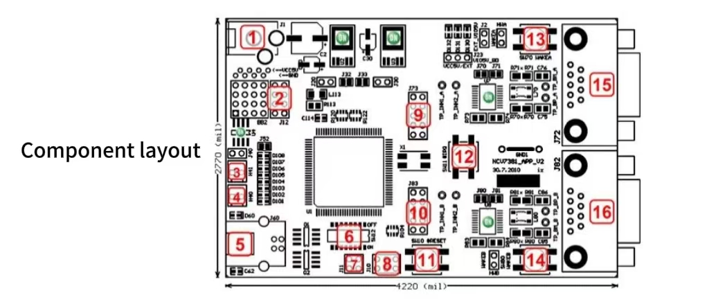
2. Try mounting decoupling capacitors near critical components such as ROM and RAM chips.
In reality, PCB routing, pin routing, and wiring can contain significant inductive effects. Large inductance can cause severe switching noise spikes in Vcc routing. The only way to prevent switching noise spikes in Vcc routing is to place a 0.1uF electronic decoupling capacitor between Vcc and the source.
If surface mount components are on the board, surface mount capacitors can directly next to the component and connected to the Vcc pin. Tile capacitors are better because they have low ESL (electrostatic discharge), high frequency impedance, and good dielectric stability over temperature and time.
Since tantalum capacitors have high impedance at high frequencies, they should not be used as many times as possible.
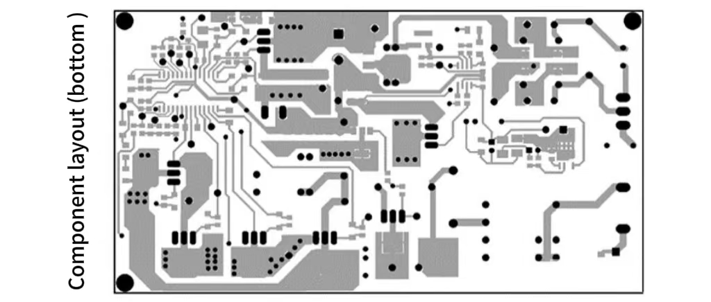
When placing decoupling capacitors in a PCBA control board PCB design, following these points:
- Connect an approximately 100uF electrolytic capacitor to the power input terminal of the printed circuit board. A larger capacitance is better if volume allows.
- Ideally, place a 0.01uF ceramic capacitor next to each IC chip. If the spacing between the PCB and the chip is too small to accommodate this, place 1-10 tantalum capacitors for every 10 chips.
- Connect decoupling capacitors between the power line (Vcc) and the ground line to handle components with weak anti-interference capabilities and large current fluctuations during shutdown, as well as storage components such as RAM and ROM.
- Capacitor leads should not be too long, especially for high-frequency bypass capacitors.
In microcontroller control systems, there are various types of ground wires, including system ground, shield ground, logic ground, and simulation ground. The rationality of the PCB design and layout of the ground wires determines the circuit board’s anti-interference capability.
When designing and connecting ground wires on a PCBA control board PCB, take following considerations into account:
- Logic and analog grounds should be wired separately and not used together. Connect their respective ground wires to the corresponding power ground wires.
In the design, analog ground wires should as thick as possible, and the grounding area at the front end should be maximized. Generally, for input and output analog signals, MCU circuits are best separated using optocouplers.
- When designing the printed circuit board for logic circuits, ground wires should form a closed loop to improve the circuit’s anti-interference capability.
- Ground wires should be as thick as possible. If the ground wire is too thin, its resistance will be high. This cause the ground potential to change with current variations, resulting in unstable signal levels and reduced anti-interference capability.
If wiring space allows, ensure the width of the main ground wire is at least 2-3 mm, and the ground wire on component pins should be approximately 1.5 mm.
- Pay attention to the choice of grounding point. When the signal frequency on the circuit board is below 1MHz, the electromagnetic induction effect between wiring and components is small, while the circulating current formed by the grounding circuit has a greater impact on interference; therefore, a grounding point should be used to avoid loops.
When the signal frequency on the circuit board exceeds 10MHz, the grounding impedance becomes very high due to the significant inductive effect of the wiring, and the circulating current formed in the grounding circuit is no longer a major issue. Therefore, multi-point grounding should for minimizing grounding impedance.
- In addition to making the power lines as thick as possible according to the current magnitude, the power lines and grounding lines should be routed in the same direction as the data lines in the cube. At the end of the routing, the grounding line should cover the bottom of the circuit board. These methods can help enhance the circuit’s anti-interference capability.
For component layout on a PCB, five suggestions:
1. Aesthetics
The component layout on a PCB should be as aesthetically pleasing as possible. Besides ensuring neat and orderly component placement, the layout design should also consider the smoothness and elegance of the traces. Often, users judge the quality of a circuit design solely by the neatness of the component layout. For the sake of product image, prioritize the former when performance requirements are not stringent. However, in high-performance applications, where the requirements for the circuit board are higher and the components are encapsulated and not normally visible, the aesthetics of the traces should be prioritized.
2. Signal Interference
Signal interference is a crucial factor to consider in PCB design and layout. Note the following aspects:
- Separate or even isolate weak signal circuits from strong signal circuits;
- Separate AC and DC sections;
- Separate high-frequency and low-frequency sections;
- Pay attention to the routing of signal lines and the placement of ground lines;
- Implement appropriate shielding and filtering measures.
3. Stress
The PCB board should be able to withstand various external forces and vibrations during installation and operation. This requires a reasonable arrangement of the positions of all holes (screw holes, irregular holes) on the board. Generally, the distance between the hole and the board edge should be at least greater than the hole diameter. At the same time, pay attention to ensuring that the weakest section of the board caused by irregular holes has sufficient bending strength. Connectors that directly “extend” out of the device housing on the board must be properly secured to ensure long-term reliability.
4. Heat
The layout of PCB board components should pay attention to the placement of high-power, heat-generating devices, ensuring sufficient heat dissipation. Especially in precision analog systems, special attention should be paid to the adverse effects of the temperature field generated by these devices on the fragile preamplifier circuitry. Generally, very high-power components should be made into a separate module, and certain thermal isolation measures should be taken between them and the signal processing circuitry.