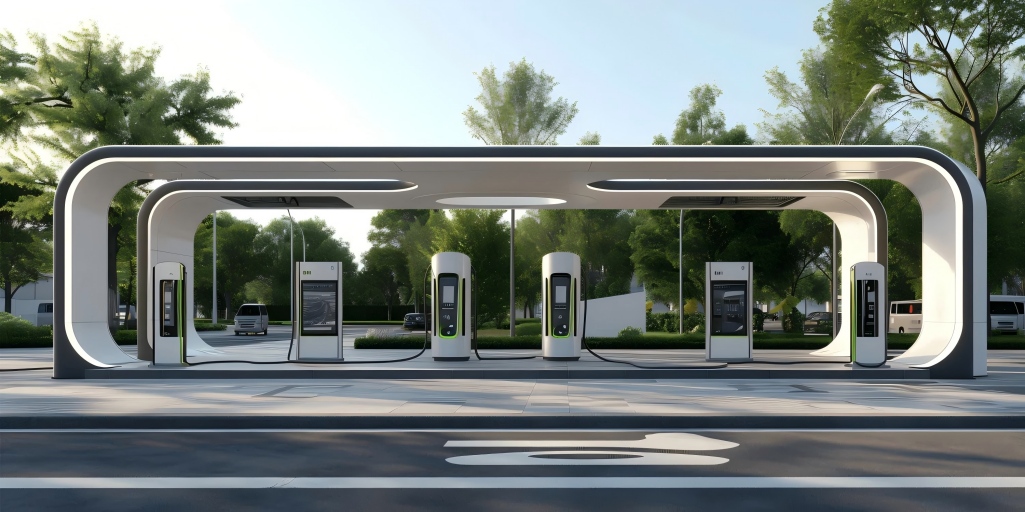
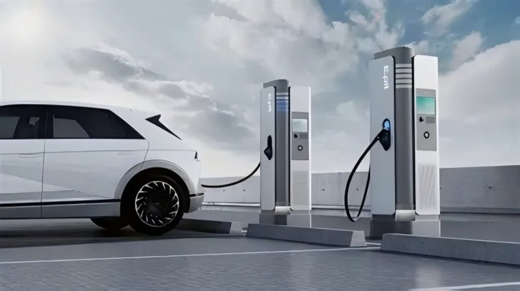
Every time you charge your electric vehicle, you rely on the onboard charger, so it must perform reliably. PCB integration technology enhances charger performance. It uses specialized materials that withstand high temperatures, preventing heat-induced damage. Metal cores and thick copper layers facilitate heat dissipation, preventing the charger from overheating. This article delves into the complexity of EV charger PCB components, highlighting their critical role in EV charging infrastructure.
Designing EV Charger PCBs
Circuit Complexity: An EV charger is inherently a complex system encompassing multiple facets. Consequently, the PCBs dedicated to these chargers bear the critical responsibility of managing charger safety and must be flawlessly precise. Circuit design must skillfully navigate intricate details to ensure the safety and reliability of the charging process.
Safety Features: To meet and exceed stringent safety standards, integrating comprehensive safety features into PCB design is paramount. These include critical components such as fuses, surge protectors, and ground fault protection mechanisms. By rigorously adhering to these principles, the PCB acts as a protective barrier, shielding users from potential electrical hazards and creating an impenetrable safety environment.
Thermal Management: The high power demands inherent in EV charging inevitably generate significant heat. Under this demanding test, effective thermal management is paramount. PCBs must exhibit exceptional heat dissipation capabilities and employ meticulously designed strategies to prevent overheating. These approaches not only extend PCB lifespan but also ensure chargers operate at peak performance.
Signal Integrity: The symbiotic relationship between chargers and vehicles relies on effective communication, which hinges entirely on the integrity of high-speed data transmission. Thus, the PCB assumes the critical role of gatekeeper, responsible for safeguarding the integrity of data exchange. To this end, noise interference emerges as a formidable adversary that must be suppressed through thoughtful design. PCB design must incorporate safeguards that effectively mitigate noise interference, thereby ensuring the reliability and efficacy of communication between the charger and the vehicle.
Manufacturing and Assembly Processes: The Core of EV Charging
1. PCB Layout
PCB layout marks the pioneering stage of the entire manufacturing process. Here, the physical blueprint of the PCB takes shape, meticulously outlining component placement, trace routing, and incorporating critical markings that serve as indispensable guides during subsequent manufacturing and assembly. It is at this stage that the PCB’s architecture is defined, laying the foundation for its future role within the EV charging system.
2. Printed Circuit Board Manufacturing
Once the PCB layout is finalized, the manufacturing process formally commences, typically outsourced to specialized factories proficient in this craft. This phase marks the transformation of a concept into a tangible product. Through an almost alchemical process, patterns are etched onto the copper-clad laminate—the substrate that will host the intricate circuits essential for the charger’s operation. The convergence of precision engineering, masterful craftsmanship, and cutting-edge technology breathes life into the nascent PCB, establishing its foundation for playing a pivotal role in the EV charging domain.
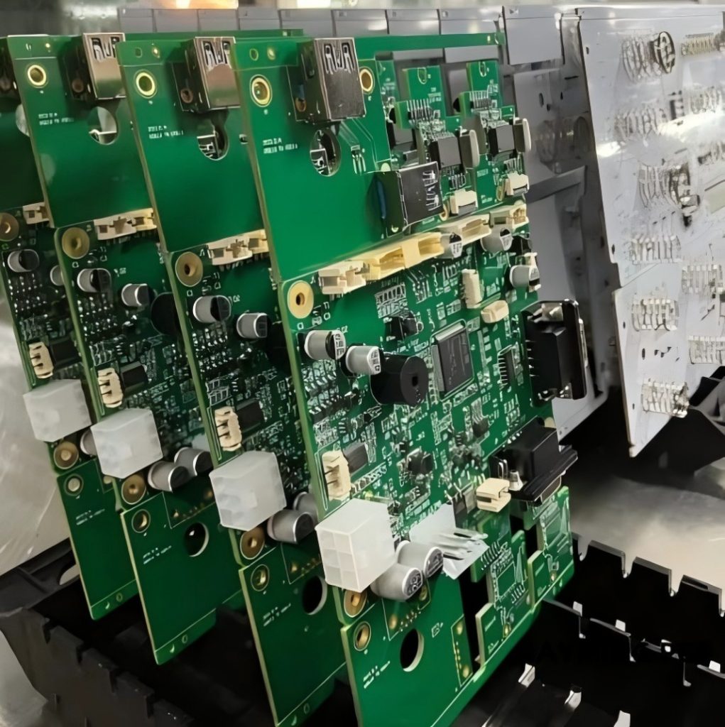
3. PCB Assembly
The assembly process signifies the fixation of electronic components onto the PCB, transforming it from an inert state into a powerful functional unit. Two primary techniques—Through-Hole Technology (THT) and Surface Mount Technology (SMT)—take center stage:
1) Through-Hole Technology (THT): In this method, components are inserted into precisely drilled holes on the PCB and soldered from the opposite side. This technique is ideal for larger components requiring additional mechanical support. The combination of mechanical integrity and electrical connectivity ultimately builds a robust foundation.
2) Surface Mount Technology (SMT): Unlike THT, SMT connects components directly to the PCB surface. This approach not only reduces overall size but also accelerates the assembly process, elevating efficiency to a critical level. Today, PCBs are densely populated with various surface-mount components, serving as a testament to precision engineering.
4. Quality Control
Within the harmonious integration of design, manufacturing, and assembly, quality control stands as the steadfast guardian of precision. Rigorous inspection, meticulous alignment verification, and solder joint evaluation form the essential journey for every PCB. These stringent quality control measures ensure the safety and functionality of the final product, guaranteeing that each rigorously tested EV charger PCB exemplifies excellence.
Testing Procedures: Ensuring Excellence and Safety
Electrical Testing
The core of electrical testing lies in verifying the PCB’s conductivity—a prerequisite for proper operation. This phase involves a thorough examination of circuit continuity, akin to meticulously inspecting a biological organism’s circulatory system. Every path, connection point, and junction undergoes a detailed assessment to guarantee unimpeded current flow throughout the PCB. Any anomalies or interruptions in the circuit are identified and rectified during this phase, guaranteeing the PCB’s electrical integrity meets standards.
Functional Testing
The true capabilities of a PCB are revealed through rigorous functional testing. Here, the PCB undergoes a series of tests that extend beyond continuity to probe the essence of its intended use. Performance testing determines whether the PCB can function effectively within the broader ecosystem of EV chargers. Parameters, specifications, and performance requirements undergo rigorous scrutiny. Only when the PCB emerges unscathed from this arduous challenge can it be entrusted with powering EV charging systems.
Safety and Compliance Testing
1) High Voltage Test (Hipot): During this test, the PCB undergoes high-voltage evaluation to verify its ability to withstand elevated potentials without leakage or breakdown. This is a test of the PCB’s resilience, ensuring it can withstand the rigors of high-voltage surges.
2) Environmental Testing: The PCB must undergo rigorous evaluation of its ability to withstand various environmental conditions. It must endure temperature fluctuations, humidity changes, and other environmental challenges to ensure stable operation in real-world scenarios.
3) EMC Testing (Electromagnetic Compatibility): In the increasingly interconnected world of EV charging, the PCB’s ability to coexist harmoniously with other electronic systems is critical. EMC testing evaluates the PCB’s capability to operate without generating electromagnetic interference or being affected by external electromagnetic disturbances.
4) Compliance with Safety Standards: This PCB meets a series of safety standards, including IEC 61851, ISO 15118, SAE J1772, and IEC 62196. This ensures compliance with the highest industry benchmarks and provides recognition for its safety and reliability.
Conclusion
In summary, the assembly of printed circuit boards (PCBs) for EV chargers is critical to the successful operation of EV charging systems. Lensuo understands the importance of this process and possesses comprehensive PCB assembly equipment to meet your needs.


