In the PCB manufacturing industry, terms like “through via”, “blind via” and “buried via” are everywhere—especially in high-density board designs.
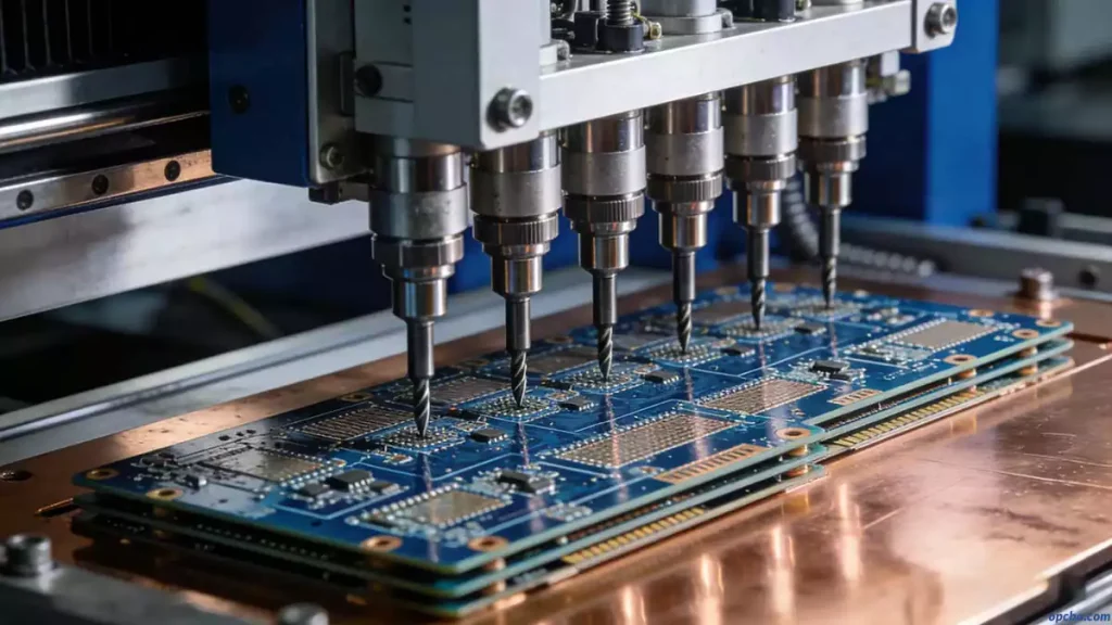
PCB drilling is the process of creating holes on the board surface to connect circuits between layers, a critical step that directly impacts interconnection reliability.
Common PCB Via Types (and Their Uses)
Understanding PCB via types is key to choosing the right drilling method for your design. Not all vias serve the same purpose, and mixing them up can lead to production issues.
Through-Hole (Via)
This type only handles electrical conduction and doesn’t require component soldering.
The surface can be windowed (pad exposed), covered with solder mask, or plugged with ink—depending on the design requirements.
Plug-in Holes (Pad Holes)
These holes are for inserting component pins, so the pad surface must be fully exposed to ensure strong soldering adhesion.
In real production, misaligned plug-in holes are a common defect that causes component installation failures.
Non-Plated Through Holes (NPTH)
Also called mounting holes, these are used for screws or plastic component feet.
They have no electrical properties and serve only as positioning and fixing points for the PCB.
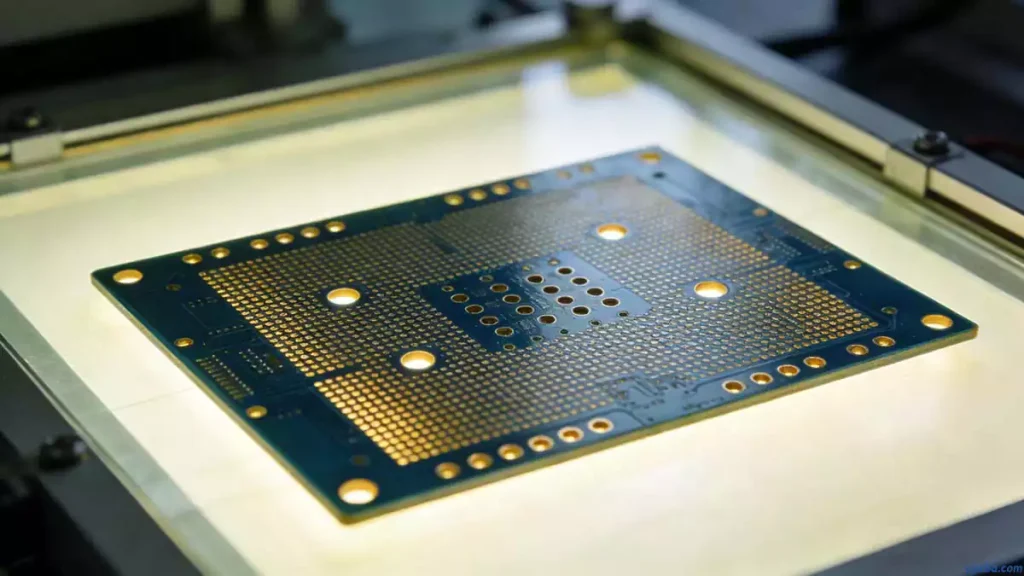
Plated Through Holes (PTH) vs. NPTH
Plated Through Holes (PTH) are conductive, carrying signals to connect different board layers and securing components during assembly.
Non-Plated Holes (NPTH), by contrast, are non-conductive and strictly for mechanical fixing.
PCB Drilling Process Classification
Based on manufacturing techniques, PCB drilling falls into two main categories—each with its own strengths and ideal use cases.
Through-Hole Drilling
These holes penetrate the entire board, used for internal interconnections or component mounting positioning.
They’re relatively easy to process and cost-effective, making them the most common choice for standard PCBs.
Blind Via Drilling
Blind vias are located on the top or bottom surface of the PCB, with a specific depth.
They connect surface circuits to inner layers below, and their depth usually doesn’t exceed a certain ratio relative to the hole diameter.
They’re ideal for high-density PCBs where space is limited.
Buried Via Drilling
Buried vias are hidden in the inner layers of the PCB, never extending to the board surface.
They’re used for internal layer interconnections, helping to save surface space but requiring more precise drilling control.
PCB Drilling Technology
Two core technologies dominate modern PCB drilling: mechanical and laser drilling.
Choosing the right one depends on hole size, material, and cost—something we see PCB manufacturers grapple with daily.
Mechanical Drilling
Mechanical drilling is straightforward but less precise, with a minimum hole diameter of around 6 mils (0.006 inches).
When used on softer materials like FR4, drill bits can handle up to 800 hits before needing replacement.
For denser materials, that number drops to 200 hits.
Choosing the wrong drill for the material often leads to PCB scrap and higher manufacturing costs.
Laser Drilling
Laser drilling is a non-contact process—no physical tool touches the workpiece.
A laser beam removes board material to create precise holes, with controlled depth and a minimum diameter of just 2 mils (0.002 inches).
It’s the go-to for high-precision, high-density PCBs where small holes are critical.
Mastering PCB drilling technology is essential for producing reliable, high-performance PCBs—whether for standard or high-density designs.
For more details about PCB drilling processes or custom PCB fabrication, visit opcba to discuss your project needs.


