As we all know, computers and mobile phones rely on printed circuit boards (PCBs). These boards act as core electrical connection providers for electronic components. To create a custom electronic PCB, you need to follow a clear, efficient workflow. Let’s explore how to custom electronic board PCB from design to delivery.
1. Core Step 1: Design the PCB Schematic
Designing a PCB schematic is the foundational first step of custom electronic PCB production. Industry-standard tools like Eagle PCB streamline schematic capture and layout work—learn more about What is Eagle PCB? to optimize your design process. This process centers on two key factors: the electrical performance of each component and practical manufacturing needs.
A well-designed schematic accurately reflects the PCB’s core functions and the connection relationships between all components. It is the blueprint for the entire PCB production process. After manufacturing, comprehensive testing of the circuit board is essential. If issues arise during testing, you can trace the root cause using the initial schematic. You may then re-solder components or replace faulty parts. Only after successful testing is the custom electronic PCB fully completed.
2. Core Step 2: Partner with a Qualified PCB Manufacturer
Once the PCB schematic is finalized, the next critical step is to select a suitable PCB manufacturer. You will need to send your completed Gerber files (the standard design file format for PCBs) to your chosen supplier.
If you plan to produce a PCBA (Printed Circuit Board Assembly), you must also provide the supplier with detailed BOM (Bill of Materials) information. Alternatively, you can ship purchased electronic components to the manufacturer’s facility. This ensures smooth SMT (Surface Mount Technology) processing and efficient completion of the assembly process.
For most customers, custom electronic board PCB only requires these two core steps: schematic design and manufacturer collaboration. Below is a detailed breakdown of the standard double-sided PCB production process.
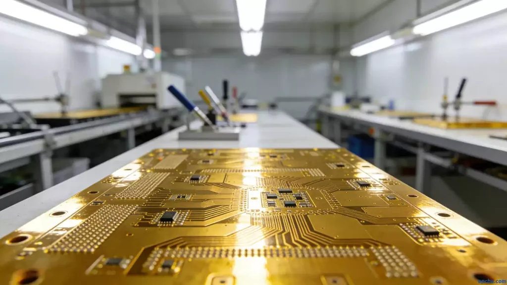
Step-by-Step Double-Sided PCB Production Process
(1) MI Cutting (Material Cutting)
Based on the customer’s manufacturing specifications, large PCB panels are edge-cut and trimmed into small, customized board sizes. This step shapes the PCB to meet the final product’s space and form factor requirements.
(2) Drilling & Hole Metallization
Drilling is the first production step for circuit boards. Manufacturers drill holes of varying diameters (via holes, electrical holes, mechanical holes) at customer-specified positions on the cut panels.
Next comes hole metallization (copper deposition). Chemical methods are used to deposit a thin layer of copper on the inner walls of insulating holes. This forms a conductive layer, laying the groundwork for subsequent circuit connection.
(3) Circuit Fabrication & Plating
This phase includes three key sub-steps plus AOI inspection:
- Lamination: Blue photosensitive film is applied to both sides of the PCB panel.
- Exposure: Using an automatic exposure machine, the circuit areas are exposed to light (the circuit regions appear black in the film).
- Development: The exposed panel is treated with developer to remove the film from circuit areas, exposing the underlying copper foil.
- Graphic Electroplating: A thicker layer of copper and tin is added to the exposed copper foil. The film is then removed using a film-stripping solution.
- Etching: The panel is etched to remove unplated copper (tin acts as a protective layer). Finally, tin is stripped using a tin-stripping solution.
- AOI Optical Inspection: An optical detector checks the semi-finished PCB. It identifies short circuits, open circuits, and other defects, which are repaired promptly to ensure quality.
(4) Solder Mask Coating
At this stage, the PCB is a semi-finished product. Solder mask coating involves applying a protective layer (most commonly green oil) to the board’s surface. This layer shields the copper from oxygen and prevents oxidation, which would degrade the PCB’s performance and service life.
(5) Silk Screen Printing
Custom text and markings are printed on the PCB via silk screen printing. This includes component codes, part names, model numbers, and other customer-specified labels for easy identification during assembly and maintenance.
(6) Surface Finishing
Two common surface treatment methods are used for custom PCBs: immersion gold (ENIG) and hot air solder level (HASL). For high-power or heat-sensitive applications, specialized substrates like Aluminum PCB pair with these finishes to deliver superior thermal management. Immersion gold produces gold-plated boards, while HASL results in silver-finished boards. Both treatments prevent copper oxidation and facilitate reliable soldering of electronic components in later stages.
(7) Final Quality Testing
After all production steps, the finished PCB undergoes manual and electronic testing. This final inspection verifies the board’s electrical functionality, component compatibility, and overall quality to ensure it meets customer specifications.
(8) Shipment
Qualified PCBs are packaged and shipped to the customer, completing the custom electronic PCB manufacturing process.
Your Trusted Partner for Custom Electronic Board PCB
opcba.com specializes in custom electronic board PCB manufacturing for a wide range of applications, from consumer electronics to industrial devices. We offer end-to-end support, from schematic design review to final PCB delivery. If you’re searching for a reliable PCB manufacturer for your custom project, email our team for a personalized quote and technical guidance today.


