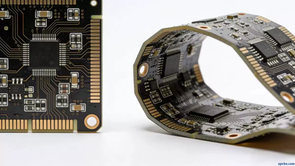
What Is PCB Board Warp & Its Related Damage
First of all, PCB board warp refers to the bending or deformation of a printed circuit board. Notably, it is a common defect in PCB manufacturing and assembly, and can bring serious problems to production and use.
Damage Caused by PCB Board Warping
In automatic surface mounting lines, a warped PCB cannot accurately position itself. Furthermore, components cannot be inserted or mounted correctly onto board holes or surface pads. Consequently, this may even damage automatic insertion machines.
PCB boards with components will bend after soldering. In addition, component pins become hard to cut evenly and neatly. Moreover, warped boards also cannot be installed into chassis or internal sockets. As a result, this creates major problems for assembly plants.
Modern surface mount technology is developing toward high precision, high speed and intelligence. Consequently, it has higher requirements for the flatness of PCBs, which act as the carrier of electronic components.
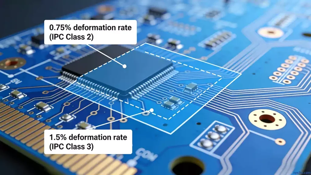
Specifically, the IPC standard clearly specifies the allowable deformation rate:
- 0.75% for PCBs with surface mount devices
- 1.5% for PCBs without surface mount devices
To meet high-precision mounting demands, many electronic manufacturers apply stricter standards. For example, some require a deformation rate of 0.5%, and a few even limit it to 0.3%.
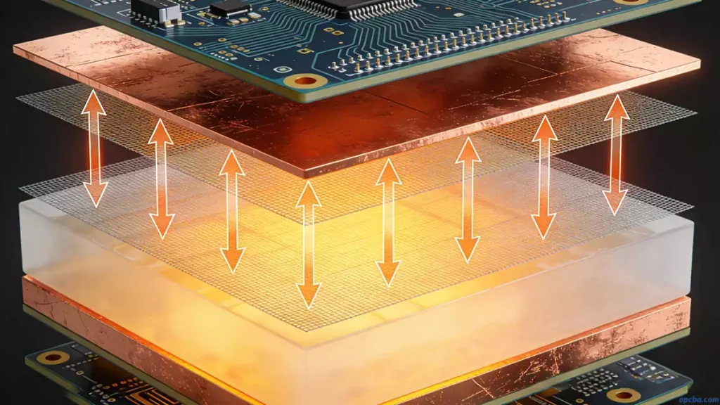
PCB boards consist of copper foil, resin, glass cloth and other materials. Furthermore, these materials have different physical and chemical properties. Consequently, thermal stress remains after lamination, which easily leads to deformation.
In addition, high-temperature treatment, mechanical cutting and wet processing during PCB manufacturing also affect board warping. Overall, the causes of PCB deformation are complex and diverse. Therefore, reducing warpage has become a key challenge for PCB manufacturers
Main Causes of PCB Board Warp
PCB deformation relates to materials, structure, layout, processing and many other factors. To break this down, below are the most common causes.
1. Uneven Copper Distribution
First, large-area copper foils are often designed for grounding or power layers. If these copper areas are unevenly distributed, the board will absorb and dissipate heat at different speeds.
This inconsistent heating and cooling creates internal stress. Furthermore, when temperature exceeds the Tg value, the board softens and warps.
2. Via Restrictions
Next, vias connect different layers of multilayer PCBs. They act like mechanical rivets and limit the expansion and contraction of the board. Consequently, this restriction indirectly causes bending and warping.
3. Board Weight & Size
Third, overweight components or an overlarge board size can cause sagging. In a reflow oven, chains support the board only on both sides. As a result, heavy boards will bend in the middle due to their own weight.
4. V-Cut Depth & Connecting Strips
Fourth, V-Cut cuts grooves into the panel and weakens the board structure. Notably, improper V-Cut depth and connecting strip design are major causes of board deformation.
5. Material & Lamination Factors
Fifth, manufacturers laminate PCBs with core boards, prepregs and outer copper foils. Each material has a different coefficient of thermal expansion (CTE).
For example:
- Copper foil CTE: about 17×10⁻⁶
- FR-4 CTE below Tg: 50–70×10⁻⁶
- FR-4 CTE above Tg: 250–350×10⁻⁶
Consequently, thermal deformation occurs during lamination due to CTE differences.
6. Processing & Thermal Stress
Sixth, PCB processing creates both thermal stress and mechanical stress. Specifically:
- Thermal stress mainly comes from the lamination process
- Mechanical stress comes from stacking, handling and baking
Key processes that cause warping include:
- Copper Clad Laminate Material: Uneven curing during pressing leaves internal stress
- Lamination: Thicker boards and complex layouts make stress harder to eliminate
- Solder Mask & Baking: Temperatures above Tg make boards soft and easy to deform
- Hot Air Solder Leveling: Sudden heating and cooling creates strong thermal stress
- Improper Storage: Vertical insertion or tight stacking causes mechanical deformatio
How to Prevent PCB Board Warp
Overall, PCB warping seriously affects assembly and final use. Therefore, effective prevention must be applied in design, production and storage.
1. Engineering Design Improvements
First, engineering design improvements include:
- Keep interlayer prepreg arrangement symmetrical
- Use core boards and prepregs from the same supplier
- Balance copper area on both outer layers; add grids if one side is too sparse
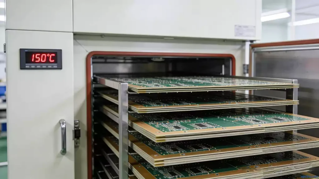
2. Pre-Baking Before Cutting
Second, pre-bake copper clad laminates at 150℃ for 8±2 hours. This removes moisture, fully cures resin and releases residual stress.
3. Distinguish Prepreg Warp & Weft Directions
Third, prepreg has different shrinkage rates in warp and weft directions. Mixing directions will cause serious warping after lamination.
4. Stress Relief After Lamination
Fourth, after hot and cold pressing, place boards flat in an oven at 150℃ for 4 hours. This slowly releases internal stress.
5. Straightening for Thin Plates During Plating
Fifth, use special fixtures for ultra-thin boards (0.4–0.6mm) during electroplating to avoid bending.
6. Proper Cooling After Hot Air Leveling
Sixth, cool boards naturally on a flat surface after soldering. Avoid sudden cold water shock, which causes warping and delamination.
7. Rework Warped Boards
Seventh, bake unqualified boards at 150℃ under pressure for 3–6 hours. Repeat if necessary. Notably, boards with severe damage may need to be scrapped.


