If you’re an engineer working on HDI circuit boards, you know how tricky they can be—high precision, tight space, and zero room for error. HDI PCBs are everywhere these days, from smartphones to aerospace gear, and the key to getting them right? Sticking to industry standards and using practical design tricks that actually work in real projects. I’ve been designing HDI boards for years, so today I’m sharing the core IPC standards you can’t ignore, plus the blind via and stackup tips that’ll save you time and headaches.
Before We Dive In: The IPC Standards You Actually Need to Care About
Let’s be real—designing HDI without following IPC standards is a recipe for disaster. Either your board won’t pass production, or it’ll fail in real-world use. IPC (Association Connecting Electronics Industries) has four key standards specifically for HDI. Here’s what they actually mean—no jargon, just the useful parts.
1. IPC/JPCA-2315
Think of this one as your HDI cheat sheet. It’s not super technical, but it gives you a clear model to estimate design density right from the start. I use it every time I begin a new project—just plug in your requirements, and it helps you figure out if your HDI layout is feasible before you waste time on something that can’t be built. Consider it a reality check before you dive deep into routing.
2. IPC-2226
If you’re working with micropores (and let’s face it, all HDI designs do), this standard is your best friend. It doesn’t just list rules—it walks you through how to form micropores, choose the right wiring density, set design rules, and pick suitable materials and interconnection structures. The whole point is to make sure everyone’s on the same page with micropore technology, so your design is consistent and manufacturable. No more guessing if your micropore size is right—this standard tells you exactly what to do.
3. IPC-4104
This one’s all about materials. HDI needs thin, specialized materials, and IPC-4104 spells out exactly what’s acceptable. It uses a slash notation to define these thin materials and breaks them into three simple categories—so you don’t have to dig through endless material datasheets:
- Dielectric Insulator (IN): The non-conductive stuff that keeps layers separate
- Conductor (CD): The metal traces and pads that carry signals
- Conductor and Insulator (CI): Composite materials that do both
I always pull up this standard when picking materials—choose the wrong one and your signal integrity goes out the window. Don’t skip this step. (If you’re working with common substrate materials, you might also want to check out our guide on What is FR-4? The PCB Industry Standard & Its Limitations or the difference between aluminum substrate PCB and FR-4 for context on material choices.)
4. IPC-6016
Once your HDI board is designed, how do you know it’s good? IPC-6016 has the answers. It covers all the performance requirements and certification criteria for HDI structures—electrical performance, mechanical durability, and how it holds up in harsh environments. If your board meets this standard, you can ship it with confidence.
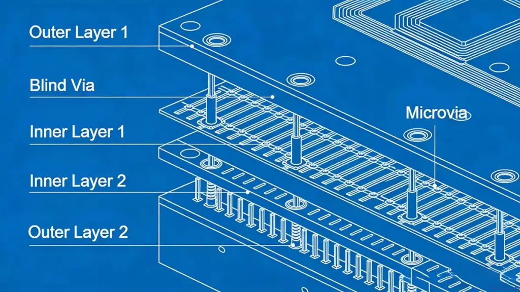
Blind Vias: The Secret to More Routing Space (My Go-To Techniques)
Blind vias are what make HDI possible—they let you route more traces in tight spaces, which is crucial for high-I/O components like BGAs. Over the years I’ve tried a lot of techniques, and these are the ones that actually work in real projects (no theoretical fluff).
1. Move Blind Vias to Free Up Space
Here’s something a lot of engineers miss: blind vias don’t have to sit in a fixed spot. You can shift them—or “swing” them, as I like to say—in the XY plane or at an angle to create extra routing room. I also place blind vias on inner layers whenever I can (3D placement, if you want the fancy term). That simple move opens up even more breakout space for BGAs.
Another trick: adjust the center distance of inner-layer blind vias. Even small changes here can give you just enough room to fit one more trace, and in dense designs, that one trace makes all the difference.
Pro tip: Use these techniques near the primary side of the board, and you’ll free up space under the secondary-side BGA or for decoupling capacitors. Trust me—that extra space will save you from re-spinning your design later.
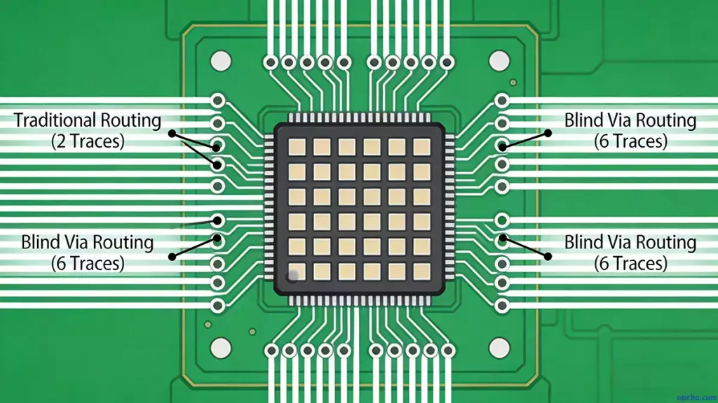
2. Blind Vias for BGA Fan-Out (Total Game-Changer)
BGAs are a pain to route—no argument there. But blind vias make them manageable. By placing blind vias between through-holes, you effectively double the routing space on inner layers.
Let me give you a real-world example: with a 1.0mm BGA, you can only fit 2 traces between through-holes on the surface. Add blind vias, and that number jumps to 6—that’s 30% more routing capacity. When you’re dealing with high-I/O BGAs, that’s huge.
I also arrange blind vias in what I call “boulevards”—tree-lined, L-shaped, or diagonal patterns—depending on where the power and ground pins sit. And if you’re working with FPGAs, reprogramming the power and ground pin positions can make this even more efficient. Small tweaks, big results.
3. Micropore Tips for BGA Pads (Don’t Make This Mistake)
When you’re using micropores for BGA fan-out, you have three options: place them outside the BGA pad, partially on the pad (partial VIP), or fully on the pad (VIP). But here’s the mistake I see new engineers make all the time: putting a through-hole dead center in a BGA pad.
If you do that—and leave it unfilled—here’s what happens during reflow: the solder melts, the BGA ball drops, and it traps air like a cork in a bottle. Total disaster.
Instead, place the through-hole off-center (eccentric). That way, air can escape as the solder flows into the micropore, and you won’t end up with soldering defects. I learned this one the hard way—don’t repeat my mistake.
HDI Stackup: Don’t Overcomplicate It (Simple Tweaks, Big Gains)
Stackup design is another area where engineers tend to overcomplicate things. You don’t need some exotic stackup to get good performance—just a few simple layer placement tweaks can make a huge difference.
The One Stackup Tweak That Saves Time (And Cuts EMI)
Here’s what I do: move the GND plane (usually the second layer) to the surface. This eliminates all those GND through-holes that eat up valuable space. Then move the PWR plane to layer 2—now you can replace through-holes with blind vias.
Compared to traditional microstrip stacks, this one change gives you four big advantages:
- Fewer manufacturing issues: No thin lines on the surface to plate or etch
- Way less EMI: A continuous GND pour on the surface acts like a Faraday cage
- Better signal integrity: The PWR layer (layer 2) sits closer to the GND layer (layer 1), which increases planar capacitance and lowers PDN inductance
- Fewer decoupling capacitors: The planar capacitance stores energy that’s easily transferred to components—you’ll need way fewer caps
Stick to the Standard Stackups
You don’t need to reinvent the wheel. IPC has three standard stackups (Type I, II, III) that are widely used to reduce through-hole counts. The dielectric between the first and second layers can be conventional prepregs, laser-drillable prepregs, RCC (Resin-Coated Copper), reinforced RCC, or BC cores—just pick what works for your project and budget.
If you’re trying to cut costs, skip the IPC-Type III structure and use a “skip” from layer 1 to layer 3. Even with thin dielectrics (less than 0.005 inch / 0.125mm), you’ll still get low PS impedance and less resonance and noise.
Where Do HDI Boards Actually Get Used?
It’s easy to get buried in the design details, so it’s worth stepping back to remember why we do this. HDI boards are for high-precision, space-constrained devices—think smartphones, aerospace systems, medical diagnostic tools, industrial robots, and high-frequency communication gear.
What makes them indispensable? Simple: they handle high routing density, small form factors, and reliable performance—things that traditional PCBs just can’t do. I’ve designed HDI boards for all these applications, and the tips I shared today work no matter what you’re building.
Quick Recap (For When You’re in a Hurry)
If you’re short on time, here’s what to remember:
- Stick to the four IPC standards—IPC/JPCA-2315, IPC-2226, IPC-4104, IPC-6016. No shortcuts.
- Use blind vias strategically—shift them, place them on inner layers, and leverage them for BGA fan-out.
- Tweak your stackup—move GND to the surface, PWR to layer 2, and keep dielectrics thin.
- Never center a via in a BGA pad—always go eccentric unless you enjoy rework.
And if you get stuck? Don’t overthink it. Our team at OPCBA has made all the mistakes so you don’t have to. Feel free to reach out if you have questions about BGA fan-out, stackup choices, or material selection—we’re happy to help.


