In any switching power supply PCB design, the physical design of the PCB board is the last step. If the design method is improper, the PCB may radiate excessive electromagnetic interference, causing the power supply to work unstably. The following is a detailed analysis of the key points for each design stage.
1. PCB Design Process from Schematic Diagram to PCB
- Create component parameters
- Input schematic netlist
- Design parameter setting
- Manual layout
- Manual wiring
- Validate design
- Review
- CAM output
2. Critical Design Parameter Setup
Before laying out your board, set clear parameters to ensure safety and manufacturability.
First, adjacent conductor spacing must meet electrical safety standards. You should make this spacing as wide as possible to simplify production and improve reliability. The minimum spacing must match the operating voltage of your power supply. For low-density wiring, you can widen signal line spacing slightly; for lines with large voltage differences, keep the path short but expand the gap to prevent interference. A standard routing spacing of 8mil works well for most switching power supply PCB design projects.
Additionally, the distance from the inner edge of a pad hole to the PCB edge must exceed 1mm. This avoids pad damage during fabrication. When connecting thin traces to pads, use a teardrop-shaped junction. This shape strengthens the connection, preventing pad peeling and trace breakage.
3. Component Layout (Key to EMI Control)
In practice, even a correct circuit schematic can lead to unreliable electronics if your PCB layout is flawed. For example, two thin parallel traces placed too close will delay signal waveforms and create reflection noise at the transmission line end. Similarly, poor power and ground routing will degrade overall performance. For this reason, you must follow strict layout rules in switching power supply PCB design.
Every switching power supply has four core current loops that drive layout decisions:
- The AC loop of the power switch
- The AC loop of the output rectifier
- The input signal source current loop
- The output load current loop
Input filter capacitors charge with near-DC current and store broadband energy; output filter capacitors do the same, storing high-frequency energy from the rectifier and smoothing DC load current. Notably, the terminals of these capacitors are critical: you must connect input and output current loops only to these capacitor terminals. If you route these loops elsewhere, AC energy will radiate into your environment and cause EMI issues.
Furthermore, the power switch and rectifier AC loops carry high-amplitude trapezoidal currents with extremely high harmonics (far above the switching fundamental frequency). Their peak amplitude can reach 5x the continuous DC current, with transition times as short as 50ns. These loops are the primary EMI sources, so you must lay them out before any other traces.
To minimize EMI, place the three core components of each loop—filter capacitor, power switch/rectifier, and inductor/transformer—right next to each other. Adjust their positions to make the current path between them as short as possible.
For switching power supply PCB design, follow this optimal layout sequence:
- First, place the transformer (the core magnetic component).
- Next, design the power switch current loop.
- Then, design the output rectifier current loop.
- Finally, connect the control circuit to the AC power loops.
When laying out input/output circuits by functional unit, stick to these principles:
- Start with PCB size: overly large boards create long traces (higher impedance, worse noise immunity, higher cost), while overly small boards cause poor heat dissipation and cross-talk. The best shape is a rectangle with a 3:2 or 4:3 aspect ratio. Keep all components at least 2mm from the board edge.
- Avoid dense component placement to simplify soldering and rework.
- Center each functional circuit around its core component, arranging other parts around it to minimize leads and connections. Place decoupling capacitors as close as possible to IC VCC pins.
- For high-frequency circuits, account for component distribution parameters. For general circuits, arrange components in parallel for easier assembly and mass production.
- Align functional units with signal flow to keep signal direction consistent.
- Prioritize routing feasibility and group components with shared connections.
- Most importantly, minimize loop area to suppress radiated EMI from your switching power supply.
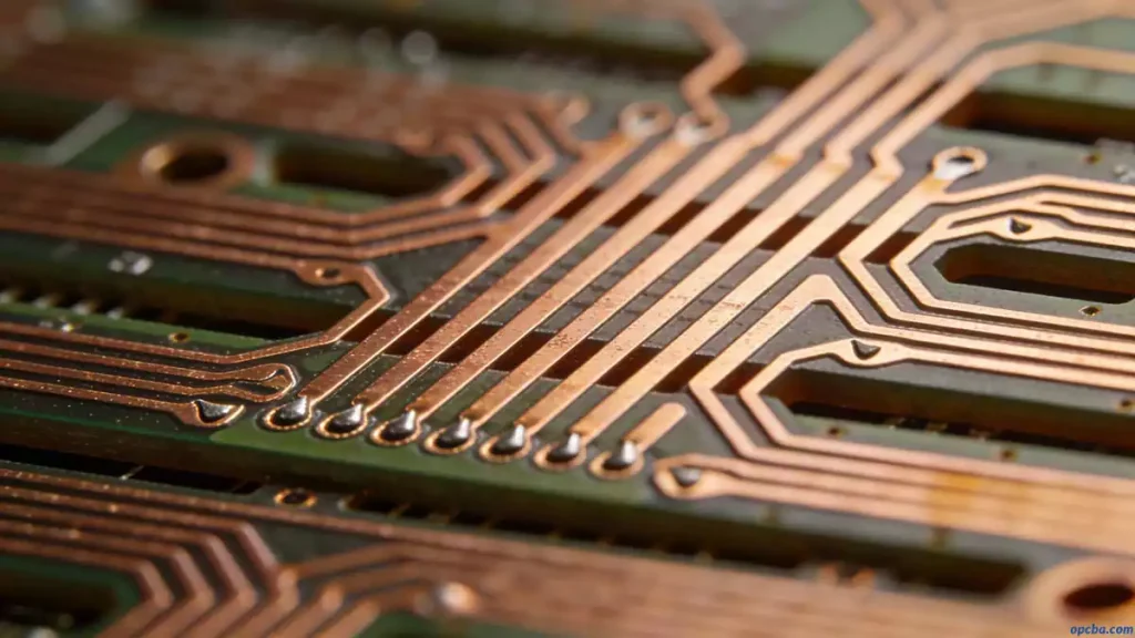
4. Wiring
Switching power supplies contain high-frequency signals, and any PCB trace can act as an antenna. The length and width of traces affect impedance and inductive reactance, thus changing frequency response. For advanced high-speed PCB layout and wiring techniques, explore our comprehensive guide: PROTEL PCB Design | High-Speed Layout & Wiring Best Practices. Even DC traces can couple RF signals from adjacent lines and cause circuit problems. Therefore, all traces carrying AC current should be designed to be as short and wide as possible, and all components connected to these traces should be placed closely.
Trace length is proportional to its inductance and impedance, while trace width is inversely proportional to them. Longer traces can transmit and receive lower-frequency electromagnetic waves and radiate more RF energy. Widen power traces according to working current to reduce loop resistance. Align the direction of power and ground traces with the current direction to improve noise immunity.
Grounding is the common reference point of the four current circuits and a key method to control interference. Mixing different ground wires will lead to unstable power supply operation.
5. Inspection
After wiring design, carefully check whether the design conforms to the formulated rules and PCB production requirements. Key inspection items include:
- Reasonableness of spacing between traces, traces and pads, traces and vias, pads and vias, vias and vias
- Appropriateness of power and ground trace width
- Opportunities to widen ground wires
Some minor errors can be ignored, such as connector outlines beyond the board frame. Rework copper laying after each modification of traces and vias.
Based on the PCB checklist, the review covers design rules, layer definition, line width, spacing, pad and via settings. It also focuses on rationality of device layout, power and ground network routing, high-speed clock network routing and shielding, as well as placement and connection of decoupling capacitors.
6. PCB Design Output
Precautions for outputting photo files:
- Output layers include wiring layer (bottom layer), silk screen layer (top and bottom), solder mask layer (bottom layer), and drilling layer (bottom layer). Also generate NC Drill files.
- When setting the silk screen layer, select outline, text and line of top/bottom layers instead of Part Type.
- Select Board Outline for all layers.
- Use default PowerPCB settings for drilling files without any changes.


