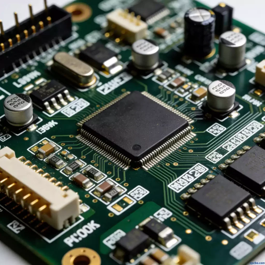
The printed circuit board (PCB) is the foundation of all electronic systems, as it dictates how components interconnect and how signals propagate across the circuit. Whether you are designing power circuits or signal circuits, PCB Layout is a critical, indispensable step in the development process. This guide covers the core rules for PCB component placement and routing, along with proven strategies to improve anti-interference performance and electromagnetic compatibility (EMC) — essential fundamentals for building robust, reliable electronic products.
1. Fundamental Rules for Component Placement
How you place components on your PCB directly impacts manufacturability, signal crosstalk, and EMC compliance. The following basic rules are essential for anyone new to PCB design:
Core Principles of Component Placement
- Functional block partitioning: Group components that serve the same function together (e.g., power supply circuitry, MCU peripheral circuits). Digital and analog circuits must be physically separated to minimize crosstalk and noise coupling.
- Reserve sufficient installation space: Do not place components within 1.27mm of non-mounting holes (e.g., positioning holes). For screw mounting holes, reserve a 3.5mm keep-out area around M2.5 screws and 4mm around M3 screws to prevent component interference during assembly.
- Avoid vias under components: Never place vias under surface-mount devices (SMDs) like horizontal resistors, through-hole inductors, or electrolytic capacitors. During wave soldering, vias in contact with component housings can easily cause short circuits.
- Maintain clearance from the board edge: The outer edge of all components should be at least 5mm away from the PCB board edge to ensure safety during handling and wave soldering.
- Keep pads and through-holes separated: Maintain a minimum 2mm gap between the outer edge of SMD component pads and adjacent through-hole pads.
- Clearance for metal components: Provide adequate spacing between metal-enclosed components (e.g., shielding cans) and other components, traces, and pads. Maintain a minimum 2mm gap between conductive elements. For positioning holes, screw holes, and slotted holes, keep them at least 3mm away from the board edge.
- Heat-generating component placement: Place heat-producing components away from heat-sensitive traces and sensitive components. Distribute high-heat components evenly across the board to avoid excessive localized temperature rise.
- Power connector placement: Locate power connectors as close to the board edge as possible. If the connector is paired with terminal wires, place the terminals on the same side. Leave sufficient space between connectors, especially soldered types, to ensure easy access for power cable plugging and unplugging.
- IC and polarized component orientation: Align all integrated circuits (ICs) in the same direction whenever possible. Clearly mark the polarity of polarized components such as capacitors and diodes. Limit the polarity orientation across the board to a maximum of two directions; if two directions are necessary, they should be perpendicular to each other.
- Uniform trace density: Maintain even trace density across the PCB. For areas with sparse routing, add grid copper pour (with a grid size greater than 8mil/0.2mm) to improve board rigidity and enhance EMC performance.
- SMD pad and via best practices: Never place vias directly on SMD pads — solder wicking through the via can cause cold joints. Avoid routing critical signal lines between connector pins.
- SMD component alignment: Align all SMD components in the same direction, with consistent silkscreen text and package orientation, to reduce errors during pick-and-place assembly.
- Unified polarity orientation: Align the positive terminals of polarized components in the same direction wherever possible to minimize the risk of incorrect placement during assembly.

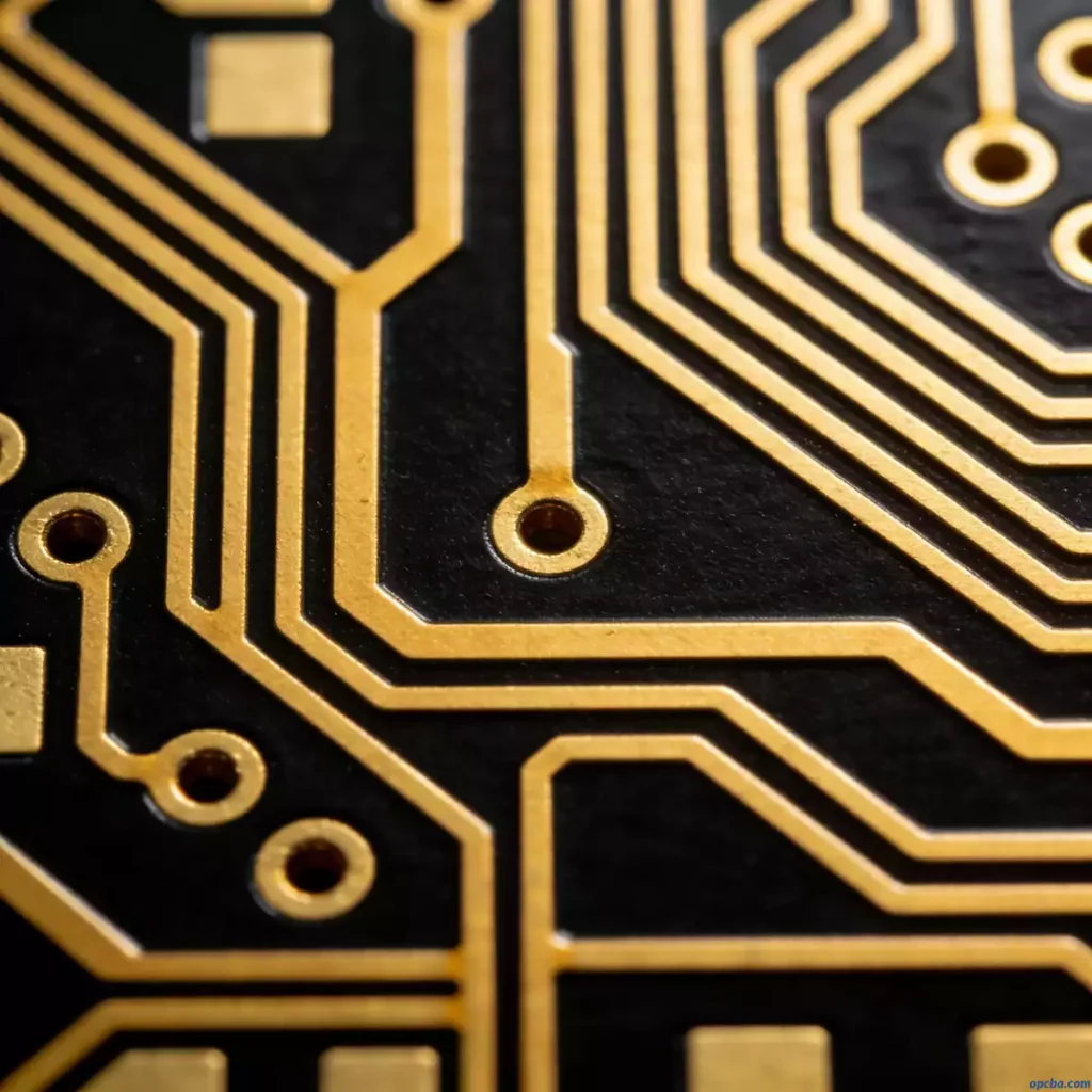
2. Key PCB Routing Design Guidelines
Trace routing directly determines the reliable operation of power and signal circuits. The following guidelines are prerequisites for ensuring signal integrity and manufacturability:
Routing and Via Specifications
- Clearance from board edges and mounting holes: Maintain a minimum 1mm clearance between traces and the PCB board edge, as well as around mounting holes.
- Trace width guidelines:
- Power traces: Should be as wide as possible, with a minimum width of 18mil, to ensure current-carrying capacity and minimize voltage drop.
- Signal traces: A minimum width of 12mil is recommended for general signal lines.
- CPU I/O traces: Can be slightly narrower, with a minimum of 10mil (8mil is acceptable for high-density layouts).
- Trace-to-trace spacing: Maintain a minimum spacing of 10mil between traces to reduce the risk of crosstalk and short circuits.
- Via size: Standard vias should have a minimum drill diameter of 30mil.
- Standard pad and hole sizes for common packages:
- DIP through-hole components: 60mil pad diameter, 40mil drill hole diameter.
- 1/4W resistors: 51×55mil pads for 0805 SMD packages; 62mil pad diameter, 42mil drill hole diameter for through-hole packages.
- Non-polarized capacitors: 51×55mil pads for 0805 SMD packages; 50mil pad diameter, 28mil drill hole diameter for through-hole packages.
- Power and ground routing: Use a radial routing topology for power and ground lines, and avoid looped paths. Minimize the length of signal traces and keep the loop area as small as possible, as smaller loops reduce radiated electromagnetic interference.
3. Strategies to Enhance PCB Anti-Interference and EMC Performance
Systems with microcontrollers (MCUs) typically pose greater EMC challenges. The following strategies are proven effective in real-world design scenarios.
Which Systems Require Extra EMC Attention?
Pay extra attention to EMC design when your system includes any of the following:
- MCUs with high main clock frequencies and high-speed bus architectures.
- High-power, high-current drive circuits (e.g., relays, high-current switches) that are prone to arcing and noise generation.
- Weak analog signal circuits or high-precision analog-to-digital (A/D) conversion circuits.
Core Anti-Interference and EMC Strategies
Select an MCU with sufficient performance, not excessive specifications
There is no need to pursue an excessively high main clock frequency. Lower operating frequencies reduce high-frequency noise and improve system stability. Keep in mind that square-wave clock signals generate far more high-frequency harmonics than sine waves, which act as noise sources that can easily radiate interference — even at low amplitudes. The most severe high-frequency noise generated by MCUs is typically concentrated around 3 times the main clock frequency.
Minimize signal transmission distortion
Most modern MCUs use high-speed CMOS technology with very high input impedance (static input current of approximately 1MΩ, input capacitance of around 10pF). Long signal traces connected to these high-impedance inputs are prone to signal reflection, distortion, and noise coupling. To mitigate this:
- Keep signal traces shorter than 25cm. Signals travel at approximately 1/3 to 1/2 the speed of light on a PCB, so a 25cm trace will introduce a 4~20ns delay.
- Limit the number of vias on a single signal trace to no more than 2.
- For high-speed signals (when the signal rise time Tr is shorter than the signal propagation delay Tpd), treat the trace as a transmission line and implement proper impedance matching.
A simple rule of thumb: The propagation delay of a signal on the PCB must not exceed the nominal delay time of the device itself.
Reduce crosstalk between signal traces
Crosstalk occurs when a signal on one trace couples into an adjacent trace. To minimize crosstalk:
- Route analog and digital signal traces separately. A solid ground plane beneath analog traces reduces characteristic impedance and minimizes signal reflection.
- Maintain a spacing between analog signal traces of 2 to 3 times their distance from the underlying ground plane.
- For highly sensitive traces, add guard traces connected to ground on both sides for shielding.
- Use a 4-layer board (with a dedicated, solid ground plane) where possible. For double-sided boards, pour copper connected to ground on the opposite side of signal traces wherever possible.
Suppress power supply noise
Power supply lines are a common entry point for conducted noise, which can easily disrupt sensitive control lines such as reset and interrupt signals. Mitigation steps include:
- Filter incoming interference from the power grid at the board’s power input (even battery-powered systems have high-frequency noise that requires filtering).
- Place a decoupling capacitor next to every IC to filter out high-frequency noise generated by the device.
- Route analog ground, digital ground, and high-power device ground separately, and connect them together at a single common ground point.
Do not overlook component characteristics at high frequencies
At high frequencies, vias, traces, and component pins introduce parasitic effects that cannot be treated as ideal components:
- A single via introduces approximately 0.6pF of parasitic capacitance.
- IC packages themselves have 26pF of parasitic capacitance; using a DIP socket adds an additional 418nH of inductance. On-board connectors introduce roughly 5~20nH of inductance.
- Traces longer than 1/20 of the wavelength of the noise signal will act as antennas, radiating electromagnetic interference.
While these effects are negligible at low frequencies, they are often the root cause of performance issues in high-speed designs.
Consider EMC during component placement
EMC performance must be considered at the component placement stage:
- Minimize the length of connecting traces between components.
- Separate analog circuits, high-speed digital circuits, and noise sources (e.g., relays, high-current switches) to avoid noise coupling.
- Place noise-sensitive circuits (e.g., A/D converters) as far as possible from noise sources (e.g., crystal oscillators, power switching devices).
Implement robust grounding and shielding
Proper grounding is the first line of defense against interference:
- For double-sided boards, use a single-point grounding topology: all power and ground return paths converge at a single common ground point.
- Route analog ground, digital ground, and high-power ground separately, and join them only at the single common ground point.
- For signals brought into the board via shielded cables: ground the shield at both ends for high-frequency/digital signals; ground the shield at one end only for low-frequency analog signals.
- Use a metal shielding can to enclose particularly sensitive circuits or high-noise sources that cannot be mitigated through other means.
Use decoupling capacitors correctly
Decoupling capacitors filter out high-frequency noise and provide instantaneous energy storage for ICs:
- Place a 0.1µF ceramic capacitor between the power and ground pins of every IC (effective for noise below 10MHz, with a typical resonant frequency around 7MHz).
- At the board’s power input, add a 1µF or 10µF high-frequency capacitor (tantalum or polycarbonate film capacitor, with a resonant frequency above 20MHz) to filter higher-frequency noise.
- Add an additional 10µF bulk storage capacitor for every 10 ICs (tantalum or polycarbonate film capacitors are recommended here as well. Standard electrolytic capacitors exhibit inductive characteristics at high frequencies, resulting in poor filtering performance).
A rough rule of thumb for selecting decoupling capacitor values is C = 1/f (e.g., a 0.1µF capacitor for a 10MHz system).
4. Field-Proven Tips to Reduce PCB Noise and EMI
The following detailed, field-proven tips from real-world PCB design practice will help you further suppress noise and improve EMI performance:
- Use slower-speed ICs where possible; reserve high-speed chips only for signals that require fast switching.
- Add a small series resistor to signal lines to slow down edge rise/fall times and reduce high-frequency noise.
- Add arc-suppression circuits to relays, high-current switches, and other inductive loads to suppress noise from arcing.
- Use the minimum necessary clock frequency; avoid overclocking beyond your system’s requirements.
- Place the crystal oscillator as close as possible to the companion chip, ground the crystal’s metal housing, surround it with a grounded guard ring, and keep clock traces as short as possible.
- Place I/O driver circuits as close to the board edge as possible to minimize trace length on the board. Implement proper filtering and series resistors for signals entering and exiting I/O ports.
- Do not leave unused MCU pins floating; connect them to VCC, ground, or configure them as outputs. Ensure all power and ground pins on ICs are properly connected.
- Do not leave unused inputs of gate circuits floating. For unused operational amplifiers, connect the non-inverting input to ground and the inverting input to the output.
- Use 45-degree angles for trace bends instead of 90-degree right angles, to reduce high-frequency signal radiation and coupling.
- Partition the board by frequency and current characteristics during placement, separating noise sources from noise-sensitive circuits.
- For single-sided or double-sided boards, make power and ground traces as wide as possible and use single-point grounding. If budget allows, use a multilayer board, which significantly reduces the inductive and capacitive parasitic effects of power and ground paths.
- Keep clock traces, bus lines, and chip select lines away from I/O lines and board connectors.
- Do not route analog voltage input and reference voltage lines adjacent to digital signals, especially clock signals.
- When using A/D chips, keep digital and analog sections within their respective areas, and avoid cross-routing between digital and analog signals.
- Route clock traces and I/O lines perpendicular to each other, not parallel, to minimize coupling.
- Keep component leads as short as possible, especially the leads of decoupling capacitors.
- Widen critical signal traces where possible, and add grounded guard traces on both sides for protection. Keep high-speed traces short and direct.
- Do not route noise-sensitive traces parallel to high-current, high-speed switching lines.
- Avoid routing traces beneath crystal oscillators or other noise-sensitive components.
- Avoid creating current loops in low-signal or low-frequency circuits.
- Minimize the loop area of signal paths; keep the loop as small as possible when a loop is unavoidable.
- Assign one decoupling capacitor per IC, and add a small high-frequency bypass capacitor in parallel with every electrolytic capacitor.
- Use tantalum or polycarbonate film capacitors for bulk energy storage, and minimize the use of standard electrolytic capacitors. Ground the housing of tubular capacitors if possible.
Final Notes
At its core, PCB Layout is meticulous work that forms a fundamental skill for hardware engineers. The rules and strategies outlined in this guide will help you design more robust PCB layouts and achieve smoother EMC compliance testing. If you encounter specific challenges in your projects, or need support with PCB prototyping, EMC testing, or design optimization, feel free to reach out to our team — we’re here to help you refine and perfect your designs.


