Printed Circuit Boards (PCBs) are essential components in modern electronics, serving as carriers for electronic parts and providing reliable electrical connections. If you are wondering how to print PCB board effectively, understanding the complete manufacturing process is key. This guide covers everything from material preparation to inner layer formation, etching, and inspection.
PCB Material Preparation and Core Materials
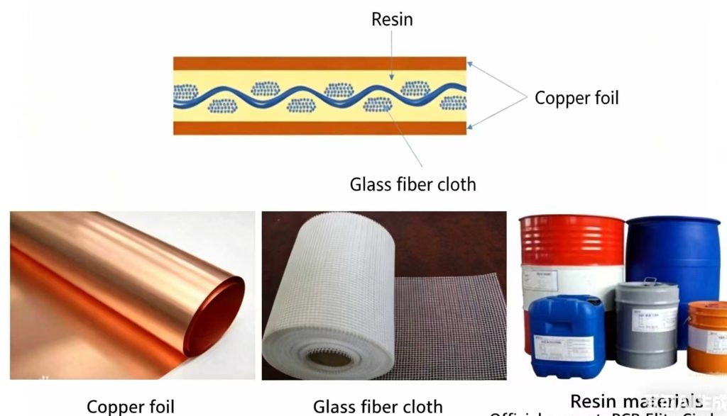
The first step in printing a PCB board is selecting the right core material. Copper-clad laminate (CCL) forms the foundation of a PCB. It consists of an insulating substrate—commonly fiberglass reinforced epoxy resin (FR-4)—and one or two layers of copper foil.
Common Types of CCL:
- FR-4: Excellent mechanical and electrical properties, cost-effective.
- High Tg Materials: Suitable for high-temperature applications.
- High-Frequency Materials: PTFE or hydrocarbon substrates for fast signal transmission.
- Metal-Based Substrates: Aluminum or copper for heat dissipation.
Key Parameters to Consider: Glass transition temperature (Tg), dielectric constant (Dk), dissipation factor (Df), heat resistance, and peel strength.
Cutting and Preprocessing PCB Panels
Before printing the PCB board, large CCL sheets must be cut and prepared.
- Step 1: Cutting. Use an automatic cutter to trim the sheets to panel sizes based on design requirements. Edges should be smooth and free of burrs to prevent damage to production equipment.
- Step 2: Edge Grinding and Chamfering. Polish the edges to remove sharp corners and fiberglass debris, ensuring smooth handling during automated processes.
- Step 3: Cleaning and Surface Roughening. Use chemical cleaning or mechanical abrasion (e.g., sandblasting) to remove oil, oxidation, and microscopic debris. This also creates a micro-rough surface that improves adhesion with dry film or liquid photoresist.
Inner Layer Pattern Transfer
Transferring the inner layer pattern is a critical step in printing PCB board. The goal is to reproduce the design circuit (usually from Gerber files) onto the copper surface with high precision.
Step 1: Applying Photoresist
- Dry Film: Laminated onto the copper surface under heat and pressure.
- Liquid Photoresist: Applied by roller, curtain, or spray coating, then baked. Suitable for fine lines.
Step 2: Exposure
Align the photomask or use laser direct imaging (LDI). Ultraviolet light or laser polymerizes the photoresist in exposed areas, making them insoluble. Unexposed areas remain removable in the developer.
Step 3: Development
Develop the board in a weak alkaline solution (e.g., sodium carbonate) to remove unexposed resist, exposing copper that will be etched. The remaining resist forms the protective circuit pattern.
Etching and Resist Removal
After inner layer pattern transfer, the next step in how to print PCB board is etching.
Step 1: Etching
Expose the developed board to acidic or alkaline etchants to remove unprotected copper, leaving the desired circuit traces intact. Controlling the etch factor ensures trace accuracy.
Step 2: Resist Stripping
Remove the remaining resist using strong alkaline solutions, revealing the final copper circuitry.
Step 3: Automated Optical Inspection (AOI)
Perform 100% AOI to detect defects like open circuits, short circuits, missing sections, pinholes, and line width deviations. This step guarantees high-quality PCB production.
Understanding how to print PCB board is essential for achieving reliable, high-precision circuits. From material selection and panel preparation to inner layer transfer, etching, and inspection, each step plays a crucial role in producing high-quality PCBs.
In the next article of this series, we will dive into outer layer processing, drilling, and PCB surface finishing techniques, exploring how these steps further enhance performance and reliability. Stay tuned to learn more about the complete PCB manufacturing process and how to achieve professional results every time.


