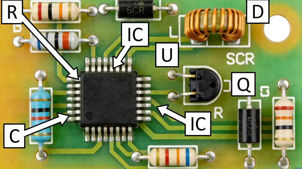
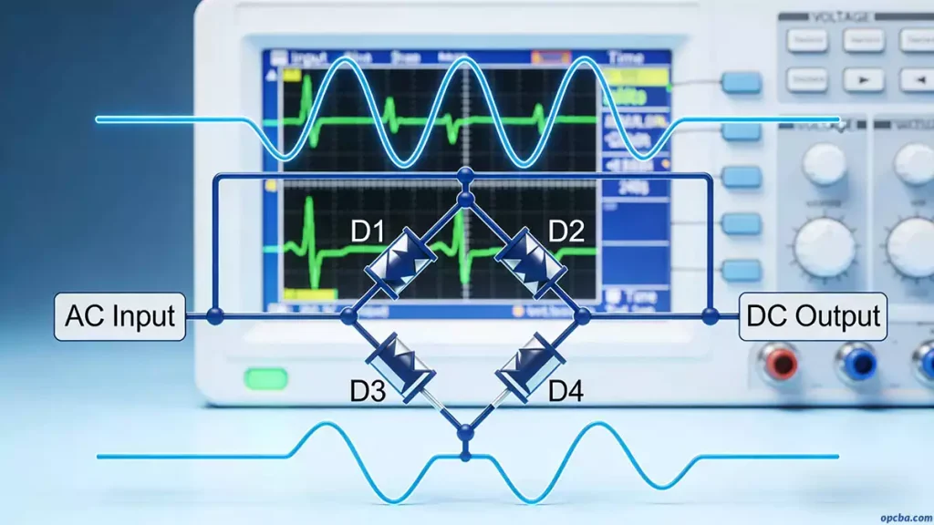
A well-designed PCB layout is the difference between a board that works reliably and one that fails in the field. Component placement and trace routing aren’t just about making connections—they determine signal integrity, thermal performance, electromagnetic compatibility, and manufacturing yield. If you’re new to core printed circuit board fundamentals and basic terminology, start with our foundational overview: Printed Circuit Board(PCB)This guide covers the practical rules that separate working boards from problematic ones. No theory for theory’s sake—just actionable guidelines you can apply in your next design. For a comprehensive, systematic deep dive into full PCB routing principles, signal integrity specifications, and advanced layout methodologies, refer to our complete guide: A Complete Guide to PCB Routing | Layout Rules, Signal Integrity & Manufacturability
Start with Component Placement—Routing Comes Second
Placement drives routing. Get the placement wrong, and no amount of routing skill will save the design. Good component placement, grouped by functional block with decoupling capacitors adjacent to IC power pins, determines roughly 70% of routing success before the first trace is drawn.
Functional zoning is the foundation. Group circuits by signal characteristics and power levels—high-speed digital, analog, high-power, and low-voltage control sections should be physically separated. Use ground planes or isolation gaps between zones. On complex boards—industrial controls, automotive systems—proper zoning directly determines whether the design passes EMC testing.
Power ICs (LDOs and DC-DC converters) belong close to their loads. Input and output capacitors sit right next to the pins. The power loop area must be minimized—this is critical. Keep inductors and diodes close, and maintain at least 5 mm of clearance from analog circuits. Decoupling capacitors? Within a few millimeters of the IC power pins. Short, wide traces. Direct connection to ground.
Crystal oscillators are a frequent failure point. Place the crystal as close as possible to the IC—ideally within 5 mm. Keep traces short, straight, and matched in length to maintain stable oscillation.

Routing Best Practices: The Rules That Matter
Once placement is done, routing begins. These are the rules that earn their keep.
Route critical signals first. Not all signals carry the same importance. High-speed clocks, RF signals, high-current power paths, and sensitive analog signals get priority. DDR signals must be length-matched before routing general-purpose I/O. Critical signals get the shortest, most direct paths.
Keep traces short. One of the most important rules of good PCB layout: keep traces as short as possible. Shorter traces mean lower inductance and resistance, which makes signals more reliable. For high-speed lines, this is non-negotiable—reflections and signal degradation increase with length.
Avoid 90° corners. Signal traces should use 45° bends or arc-shaped turns instead of right angles. Right-angle routing increases parasitic capacitance, causes impedance discontinuities, and acts as a potential radiation source.
Maintain consistent trace widths. Choose trace widths based on current-carrying capacity and impedance requirements. Ensure widths remain consistent so impedance stays controlled and signals aren’t reflected. For 1 oz copper, minimum trace width is typically ≥4 mil (0.1016 mm).
Keep analog and digital signals separate. Separate them as much as possible. Keep sensitive analog signals away from noisy digital components.
Use ground and power planes. They provide low-impedance return paths and reduce electromagnetic interference (EMI). Every signal layer must be adjacent to a continuous reference plane.
Differential Pair Routing: The High-Speed Essentials
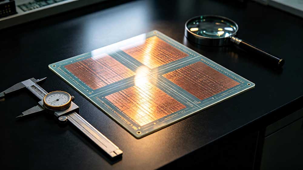
Modern high-speed interfaces—USB, PCIe, HDMI, Ethernet, SATA, LVDS—all depend on differential pairs. A differential pair is two traces carrying equal and opposite signals. The receiver reads only the voltage difference between them, which rejects common-mode noise and enables data rates from hundreds of Mbps to tens of Gbps.
Three rules dominate differential pair routing:
1. Tight, constant coupling. Route the two traces close and parallel the entire way—for example, a 5 to 10 mil gap for a 5-mil trace. The gap sets the differential impedance, so it must stay constant. Widening it around an obstacle changes the impedance and creates a reflection.
2. Match length within the pair. Intra-pair skew (the length difference between P and N) is what converts differential signal into common-mode noise. Keep it within ±5 mils for most interfaces. Compensate at each bend, not at the end of the route.
3. Share one continuous reference plane. Both traces must ride the same unbroken plane. If one trace’s reference changes, the pair goes unbalanced. Crossing a split in the reference plane is the most common high-speed routing mistake—it wrecks the return path.
Differential impedance target values:
| Interface | Target Impedance |
| Ethernet, HDMI, DisplayPort, SATA, MIPI | 100 Ω |
| PCI Express (all generations) | 85 Ω |
| USB 2.0/3.x/4, Thunderbolt | 90 Ω |
| RS-485, CAN, DDR4/5 DQS | 120 Ω |
The Return Path: The Most Overlooked Rule
Every signal consists of two paths: the signal trace and the return current flowing back. Ignoring the return path leads to signal distortion, increased crosstalk, and EMI issues.
Keep the return path close to the signal trace—minimize the loop area. Avoid crossing split ground planes. Separate analog and digital return paths. The smaller the loop area, the more stable the signal and the lower the interference.
At low speed, a trace is just a wire. Above roughly 1 Gbps—or rise times under 1 nanosecond—a trace becomes a transmission line. Sloppy routing shows up as skew, crosstalk, EMI, and failed compliance. Usually late, on hardware you have already built and paid for.
Design for Manufacturing (DFM): Don’t Skip This
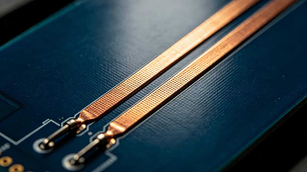
A beautiful layout that can’t be manufactured is worthless. These DFM checks catch the most expensive mistakes.
Trace width and spacing. All traces must meet the minimum width for the specified copper weight and manufacturer’s capability. All trace spacing must meet minimums for voltage rating and manufacturing capability.
No acid traps. Eliminate acute angles (<90°) in copper features where etchant can pool.
Differential pairs maintain consistent spacing. Throughout their entire length, spacing should stay within ±10% or tighter.
No traces under board edges. Keep a minimum 0.5 mm clearance from edges that will be cut during depanelization.
Impedance-controlled traces match the stackup. Verify that fab notes match the layout.
No isolated copper features. Copper islands that aren’t connected can float and cause antenna effects or ESD risk.
Via aspect ratio. For through-hole vias, board thickness divided by drill size should be ≤10:1 standard, ≤8:1 for IPC Class 3.
Stackup symmetry. The stackup should be symmetric around the midpoint—copper weight, prepreg type, and core thickness mirrored. Asymmetric stackups warp during reflow.

PCB Stackup: The Foundation
Before routing a single trace, the stackup must be right. Every signal layer must be adjacent to a continuous reference plane. Violating this principle—routing a high-speed signal between two signal layers, or over a split plane—creates EMI, crosstalk, and impedance discontinuities that no amount of termination can fully fix.
The standard 4-layer stackup is the most cost-effective controlled-impedance structure:
- Layer 1: Signal (top) — microstrip, referenced to Layer 2
- Layer 2: Ground plane — primary reference, unbroken
- Layer 3: Power plane — secondary reference
- Layer 4: Signal (bottom) — microstrip, referenced to Layer 3
This works for designs with moderate routing density and signal speeds up to 3 to 5 Gbps. For higher speeds or greater density, move to 6-layer or 8-layer stackups.
Start stackup design by identifying impedance targets and signal speed requirements, then work backward to determine layer count, dielectric thicknesses, and material grade. Coordinate with your PCB manufacturer early—they have actual prepreg thickness data and Dk values that differ from catalog specs.

2026 Trends: AI Is Changing How Boards Get Routed
PCB design is undergoing a transformation. EDA tool revenue for PCB design reached $4.2 billion in Q1 2026, marking 20 straight quarters of growth.
AI-native platforms like Quilter claim 10× faster time-to-layout compared to manual routing. Engineers using AI-assisted tools report an average 30% reduction in total design-to-tapeout time for complex multilayer designs. Cadence, Siemens EDA, and startups are deploying AI/ML tools for PCB auto-routing and DFM, cutting design cycles by 30 to 50%.
But the fundamentals haven’t changed. AI tools accelerate routing—they don’t replace the engineering judgment that decides where critical signals go, how return paths are managed, and what trade-offs to make. The rules in this guide still apply. They always will.
Summary
PCB layout and routing isn’t about connecting dots on a screen. It’s about signal integrity, thermal management, manufacturability, and electromagnetic compatibility—all balanced against cost and schedule. Good placement drives 70% of routing success. Critical signals get priority. Differential pairs demand tight coupling and matched lengths. Return paths can’t be ignored. DFM checks catch expensive mistakes before they reach production.
Get these fundamentals right, and the board works. Get them wrong, and no amount of debugging will save it.