After covering how to print PCB board inner layers in the first article, it’s time to explore the next critical steps in high-quality PCB manufacturing: lamination, drilling, hole metallization, outer layer formation, and surface finishing. These processes ensure electrical performance, mechanical reliability, and long-term durability of PCBs used in modern electronic devices.
Pre-Lamination Treatment (Black/Brown Oxide)
Before lamination, the copper surfaces of inner layers are chemically oxidized to form a uniform, dense oxide layer (black or brown). This treatment significantly improves the bonding between copper and prepreg resin, preventing delamination during high-temperature lamination or future use.
Key Benefits:
- Increased contact area for resin adhesion
- Stronger chemical bonding
- Enhanced PCB reliability
Layer Stacking and Lamination
Purpose: To align inner cores, prepreg sheets, and outer copper foils precisely and press them into a solid multilayer PCB under high temperature and pressure.
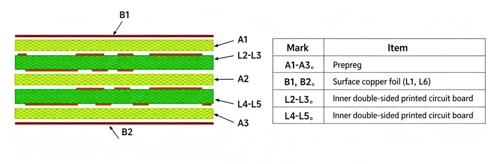
Process Details:
- Layer Stacking: Operators stack layers in the order: copper foil – prepreg – inner core – prepreg – copper foil in a controlled, dust-free environment.
- Lamination: Operators process the stack in a vacuum press with programmed heat cycles, melting and curing the resin to bond all layers into a robust, unified board.
Drilling and Hole Metallization
Drilling
Purpose: Create through-holes for interlayer electrical connections and component mounting.
Methods:
- Mechanical Drilling: High-speed tungsten carbide drills for through-holes and larger blind/buried vias.
- Laser Drilling: High-energy lasers (CO₂ or UV) create micro-blind or micro-through vias for HDI boards.
Hole Metallization (PTH & Electroplating)
Purpose: Deposit a conductive copper layer inside non-conductive holes, enabling interlayer electrical connections.
Process Steps:
- Deburring & Etching: Remove drill debris and lightly etch resin.
- Chemical Copper Deposition (PTH): Deposit 0.3–0.8 µm conductive copper chemically on hole walls.
- Electroplating: Thicken copper to 5–8 µm across the board and hole walls to ensure conductivity and mechanical strength.
Outer Layer Pattern Formation and Surface Finishing
Outer Layer Pattern Transfer
Similar to inner layers, but using pattern plating techniques. Exposed copper is plated to thicken traces, while thin unwanted copper is etched away.
Solder Mask and Legend Printing
Purpose: Protect circuits, prevent solder bridges, and provide mechanical and electrical insulation. Legends mark component positions.
Process Details:
- Solder Mask Application: Liquid Photoimageable (LPI) ink is applied, exposed (via LDI if needed), and developed.
- Curing & Legend Printing: High-temperature curing of solder mask, followed by screen printing component markings.
PCB Routing, Testing, and Final Inspection
PCB Routing
Purpose: Separate panels into individual PCBs. CNC routers or milling machines with carbide tools follow programmed paths to cut outlines and internal slots.
Electrical Testing
Flying Probe Test: High-speed probes contact test points for small batches or diverse PCB designs. Bed-of-Nails Test: Custom fixtures test all points simultaneously, ideal for mass production.
Final Visual and Quality Inspection
Automated Visual Inspection (AVI): Checks bare PCB appearance, solder mask, legends, holes, and edges.
AOI (Automated Optical Inspection): Mainly post-SMT inspection; advanced 3D AOI measures solder volume and shape quantitatively.
Mastering how to print PCB board extends beyond inner layers. Lamination, drilling, metallization, outer layer formation, solder mask, surface finishing, and testing are all critical steps that define the PCB’s reliability and performance.


