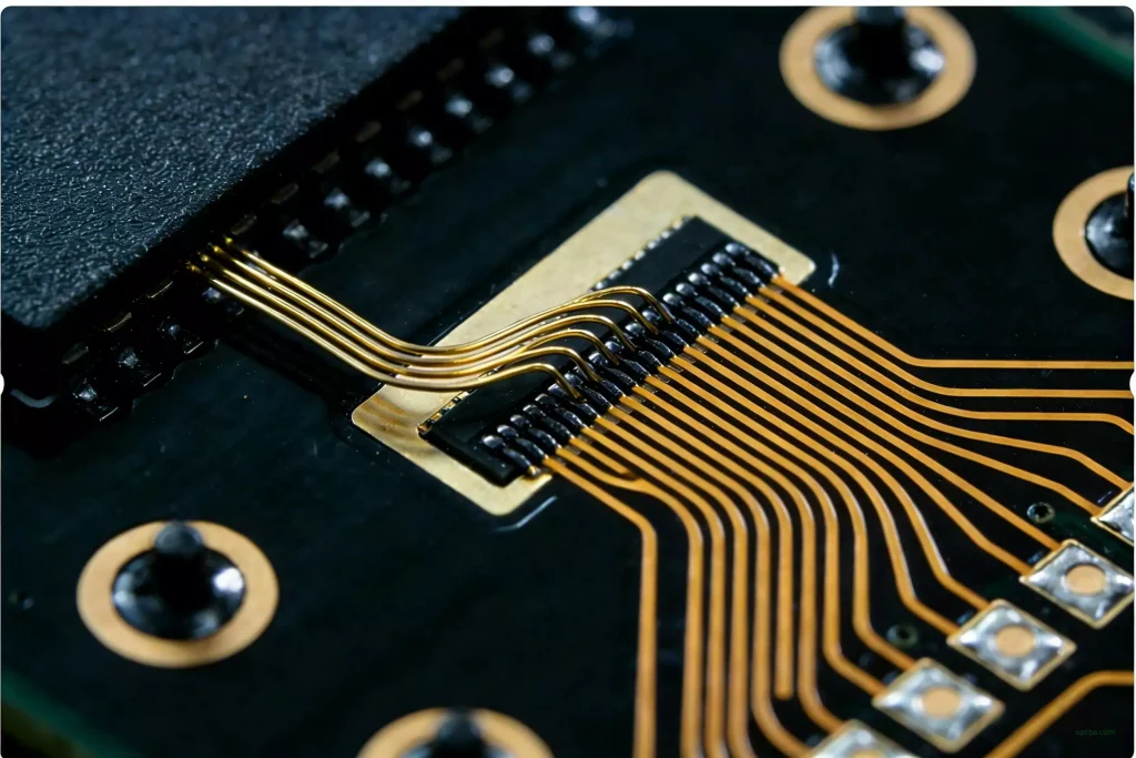
PCB routing is the process of laying out the paths that connect various devices and carry electrical signals. In PCB design, routing is a critical step in completing the product design. It can be said that the preparatory work leading up to this stage has already laid the groundwork. Throughout the entire PCB design process, the routing design phase presents the greatest challenges, requires the most meticulous skill, and involves the heaviest workload. PCB routing includes single-sided, double-sided, and multilayer routing.
Basic Principles of PCB Routing
Maintaining Signal Integrity
Signal integrity is one of the most critical considerations in the design process. It is essential to ensure that signals are not distorted during transmission due to electromagnetic interference (EMI) or crosstalk on the traces. This requires careful planning and layout, as well as strict control over factors that may affect signal quality.
Adhering to Impedance Matching Rules
Impedance matching must be taken into account during PCB routing. Different traces on the board have different characteristic impedances; if these impedances do not match, signal reflections will occur, thereby affecting signal transmission quality. Understanding and mastering the relevant impedance calculations can help designers develop better routing strategies.
Consider Manufacturing Processes During Design
When designing PCB routing, it is essential to consider the actual manufacturing processes. This includes constraints such as minimum trace width, spacing, and drill hole sizes. At the same time, designers need to anticipate potential manufacturing errors and allow for appropriate tolerance ranges in the design.
The above principles form the foundation of PCB routing and serve as important guidelines for every design phase. They ensure that electronic devices can operate stably under high-speed, high-density conditions. The following sections will further discuss PCB routing layout strategies, handling of details, and practical experience.
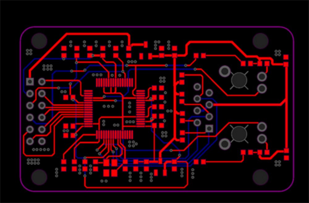
PCB Routing Layout Strategies
Pre-Layout Preparation
Preparation is crucial before proceeding with PCB routing and layout. This work lays a solid foundation for subsequent design phases.
Determine the Circuit’s Power and Thermal Analysis:
Prior to the layout phase, a detailed analysis of the circuit’s power must be conducted to predict the thermal distribution on the board. This typically involves evaluating power supply requirements, high-power-consumption components, and potentially heat-sensitive components.
The results of this analysis will guide component placement strategies, ensuring that heat-sensitive components are kept away from heat sources and that effective heat dissipation paths are designed. The design should incorporate sufficient heat dissipation measures, such as heat sinks, fans, or thermally conductive materials.
Selecting Appropriate Components and Packages:
The selection of components and packages directly affects the PCB’s size, routing difficulty, signal integrity, and thermal performance. During the selection process, factors such as component availability, cost, size, electrical performance, and package type must be considered.
When selecting components, priority should be given to those that are smaller in size and offer higher signal integrity and reliability. At the same time, it is necessary to consider compatibility among components on the board, as well as the potential for mutual interference between component pins.
Basic Principles of Layout
The fundamental principle of layout is to ensure the performance and reliability of the circuit board. The following are several core principles that must be adhered to during layout design.
Follow the Signal Flow:
The signal flow on the PCB should be as straightforward and intuitive as possible. First, define the primary signal paths, then layout the relevant components around these paths. Analog, digital, and high-frequency signals should be laid out as far apart as possible to avoid interference.
Consider Intercomponent Interference:
The degree of interference between components must be assessed, especially when routing space is limited. Sensitive analog circuits should be kept away from digital and high-frequency circuit areas. Principles of electromagnetic compatibility (EMC) should always be incorporated into the layout design to minimize interference.
Reserve Routing and Test Paths:
Routing paths should be spacious to avoid complex or overly dense routing between components. Additionally, test points and test paths should be reserved to facilitate functional testing and fault diagnosis.
Layout Optimization Methods:
Optimizing the layout can improve PCB performance and production efficiency. The following are two commonly used optimization methods:
- Reduce routing lengths through hierarchical design: It can be achieved by rationally allocating signal, power, and ground planes. Proper hierarchical planning can minimize crosstalk between signals and reduce the overall complexity of the layout through layering. During design, the hierarchical nature of signals should be considered: related signals should be placed on the same layer, and parallel routing on adjacent layers should be used to mitigate electromagnetic interference.
- Optimizing Component Placement Order and Position: The order and position of components directly affect the feasibility and efficiency of routing. Components should be sorted and positioned according to principles such as signal flow, signal type, and thermal management. During the layout process, the automatic placement features of EDA tools can be utilized to optimize component placement, combined with manual adjustments to achieve the best layout results.

PCB Routing Details
Determining Trace Width and Spacing
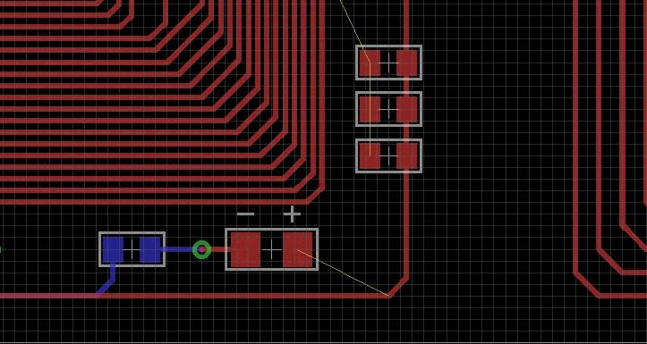
During PCB routing, trace width and spacing are two critical parameters that directly affect the board’s current-carrying capacity and signal transmission quality.
Determining Trace Width Based on Current Requirements
When current flows through PCB traces, the traces experience corresponding voltage drops and thermal effects; therefore, the trace width must be determined based on the magnitude of the current. In PCB design, the commonly used formula for calculating trace width is: [W = \frac{l}{J}\times\frac{I}{K}]
Where (W) represents the trace width, (I) represents the current flowing through the trace, (J) represents the current density (in units of A/in² or A/mm²),
and (K) represents the material coefficient, indicating the material’s thermal conductivity.
In actual design, we typically refer to the current capacity tables provided by PCB manufacturers or use the calculators built into PCB design software to determine trace width. For example, if the current flowing through a trace is 2 A and the PCB manufacturer recommends a current density of 10 A/in², the trace width can be calculated as: [W = \frac{2 A}{10 A/in²} = 0.2 in]
In multilayer boards, sufficient width must be allocated for signal and power lines on each layer to ensure safety and performance.
Adhering to Minimum Spacing Requirements for the Manufacturing Process
Minimum spacing refers to the smallest distance between traces on a PCB; it directly affects manufacturability and product reliability. Modern PCB manufacturing processes allow for very small spacings, such as 6 mil (0.15 mm), but this also results in higher manufacturing costs and increased complexity.
The size of the spacing typically depends on the PCB manufacturer’s capabilities and the PCB’s operating voltage. During design, the following factors must be considered:
- Insulation layer thickness (i.e., the PCB stackup)
- Operating voltage
- Manufacturing tolerances
Spacing must be large enough to prevent short circuits or arcing. In design software, spacing can be automatically checked and adjusted by setting design rules. In addition, potential manufacturing errors should be taken into account, which requires allowing for a certain margin of error during the design phase.
Summary
PCB routing is a core component of electronic design and directly affects circuit performance and stability. Generally speaking, standard PCB design software includes automatic routing features; however, in practice, no automatic routing tool can fully replace the skills, experience, and flexibility of a PCB layout engineer.