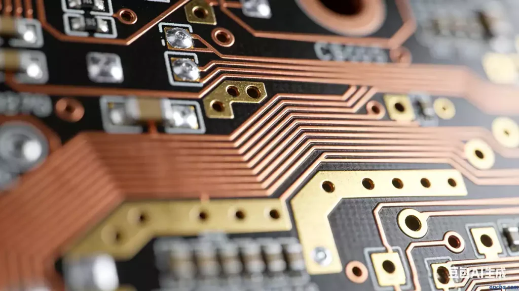
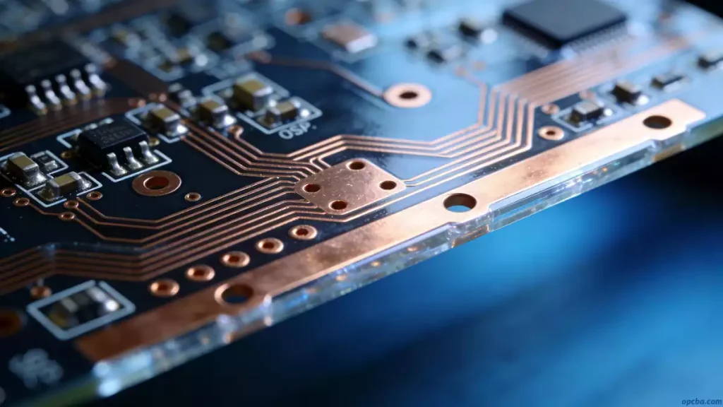
PCB surface treatments are critical for protecting copper traces, enhancing solderability, and ensuring reliable electrical connections in electronic devices. Choosing the right PCB surface treatment depends on factors like cost, storage requirements, assembly processes, and application scenarios. Below are the most common PCB surface treatments, with detailed analysis of their advantages, disadvantages, and practical applications to help you make informed decisions.
1. Bare Copper PCB Surface Treatment
Bare copper is a basic and cost-effective PCB surface treatment, widely used in simple electronic applications where short-term storage and single-sided assembly are acceptable.
Advantages: Low cost, flat surface, and excellent solderability when not oxidized. It is easy to process and suitable for low-budget projects with simple assembly requirements.
Disadvantages: Highly susceptible to acid and humidity, with very short storage life. It must be used within 2 hours after unpacking, as copper oxidizes quickly when exposed to air. It is not suitable for double-sided PCBs, as the second side will oxidize after the first SMT reflow soldering process.. For PCBs with test points, solder paste must be printed to prevent oxidation; otherwise, poor contact with test probes will occur.
2. OSP PCB Surface Treatment (Organic Solderability Preservative)
OSP is an organic film coating applied to copper traces, designed to prevent oxidation before soldering. It is a cost-effective alternative to bare copper with improved usability.
Advantages: Retains all the soldering advantages of bare copper. Expired PCBs can be reprocessed with OSP treatment to restore solderability, reducing waste. It is environmentally friendly and suitable for fine-pitch components due to its flat surface.
Disadvantages: Still susceptible to acid and humidity. The second reflow soldering must be completed within a specific time frame, and performance tends to degrade with repeated reflow. If stored for more than three months, re-surface treatment is required. As an insulating layer, OSP must be removed from test points with solder paste before electrical testing to ensure good contact with probes. The organic film only prevents copper oxidation before soldering; it evaporates when heated during soldering, allowing the solder to bond copper traces and components.
3. Immersion Gold PCB Surface Treatment
Immersion gold (ENIG) is a high-performance PCB surface treatment, featuring a thin gold layer over a nickel barrier, ideal for high-reliability and fine-pitch applications.
Advantages: Resistant to oxidation, enabling long-term storage. Its flat surface is perfect for soldering fine-pitch pins and small components. It is the preferred choice for PCBs with buttons (e.g., mobile phone PCBs). It maintains good solderability even after multiple reflow cycles and can be used as a substrate for COB (Chip On Board) packaging.
Disadvantages: Higher cost compared to other treatments. Solder strength is relatively poor, and the electroless nickel plating process may cause the “black pad” issue. The nickel layer oxidizes over time, affecting long-term reliability in harsh environments.
4. HASL PCB Surface Treatment (Hot Air Solder Leveling)
HASL is a traditional, cost-effective PCB surface treatment that coats copper traces with molten solder, then uses hot air to remove excess solder for a smooth finish.
Advantages: Low price and excellent solderability, making it suitable for general-purpose electronic products. It is easy to process and widely used in consumer electronics and industrial controls.
Disadvantages: Poor surface flatness, making it unsuitable for fine-pitch pins and small components. Solder beads are likely to form during processing, which can cause short circuits in fine-pitch component assembly. For double-sided SMT processes, the second side’s solder may re-melt during high-temperature reflow, forming spherical solder points due to gravity, resulting in uneven surfaces and soldering issues. For a detailed side-by-side analysis of ENIG (Immersion Gold) and HASL PCB surface finishes, including their performance, cost, and application suitability, read our guide: ENIG vs HASL: PCB Surface Finish Comparison.
Choosing the right PCB surface treatment is key to ensuring product reliability and reducing manufacturing costs. Contact opcba to get custom PCB fabrication with your preferred surface treatment, tailored to your project’s unique requirements.


