PCB manufacturing follows a clear, practical workflow from design validation to finished board production. Even minor process errors can cause circuit defects and reduce overall product stability.
Let’s walk through the core of the PCB manufacturing process, step by step, with details we use daily in the shop.
Design & DFM Checks
We start with the customer’s PCB design, built in tools like Altium Designer, KiCad or Cadence Allegro. Before sending files to production, we run a full DFM (Design for Manufacturability) check with Valor NPI software.
This catches issues like 0.075mm line widths (our minimum process limit is 0.1mm), undersized drill holes, or blocked solder mask bridges. Last quarter we had a batch of boards where the customer’s Gerber had unplated holes in high-density areas—we caught it in DFM and avoided a full scrap.
Turning the Design into Photo Tools
Once the design is locked, we output Gerber files to an ORC laser photoplotter to create film negatives for each layer. Each film is aligned using fiducial marks, with our plotter holding alignment accuracy within ±10μm.
Films are stored in a 22℃/50%RH controlled room to prevent humidity-induced warping. A single warped film can cause layer-to-layer shifts that lead to via misalignment later.
Prepping the Base Substrate
The core of the board is FR-4 glass epoxy core, fully cured with copper foil pre-bonded to both sides. Most of our jobs use 1.0mm thick core with 1oz copper foil; for high-power designs, we use 2oz foil.
Prepreg (partially cured epoxy sheets) is stacked between cores during lamination, not at this stage. The core is rigid and stable, ready for inner layer processing.
Building the Inner Copper Layers
For multi-layer boards, inner layers are processed first. We apply 25μm dry film to the copper surface, then expose it with a parallel light exposure machine. Our exposure machines hold alignment within ±25μm across the panel.
Unexposed dry film is washed away with 1% sodium carbonate solution at 30℃, leaving a hardened mask over the desired copper traces.
Etching to Define Traces
The board goes through an alkaline ammonia-copper etching line at 48℃, with spray pressure set to 2.5bar. We target an etch factor of ≥3 to ensure consistent line widths across the panel.
A few months back, we had a batch of 0.1mm line width boards where a blocked spray nozzle caused uneven etching. The affected panels had thin copper shorts between traces, so we scrapped them instead of risking assembly failures.
Verifying and Aligning Layers
After etching, we run every inner layer through an Omron automated optical inspection (AOI) machine. The scanner checks for open traces, copper shorts, and line width deviations against the original Gerber.
Panels that pass AOI are stacked using four registration holes drilled earlier. Layers with alignment deviation over ±50μm are pulled for rework before lamination.
Laminating the Stack into a Single Board
Verified cores are stacked with prepreg sheets and copper foil, then loaded into a vacuum laminating press. The press runs a standard cycle: 180℃ max temperature, 250psi pressure, 75 minutes at full temperature, then slow-cooled at 3℃/min.
Last year we had a small batch of boards where the wrong flow-grade prepreg was selected, leading to incomplete bonding. We added a step to verify prepreg lot numbers and resin flow specs before every lamination run to prevent repeats.
Drilling and Plating Vias
Boards go to a CNC drill with 120,000 RPM spindles, using carbide drill bits sized to customer specs. Feed rate is set to 0.05mm/rev to reduce bit breakage in thick panels.
After drilling, we run a desmear process with permanganate solution to remove resin smears from hole walls. This is a non-negotiable step—last year a rushed batch skipped full desmear, and 30% of the boards failed post-reflow continuity tests due to poor copper adhesion.
Vias are then electroless copper plated to form a conductive seed layer, followed by electrolytic plating to build up 20μm of copper in the holes.
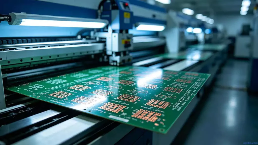
Finishing the Outer Layers
Outer layers go through the same dry film and exposure process as inner layers. After developing, we electroplate tin over the exposed copper traces, which acts as an etch resist.
Panels are then run through a second etching line to remove excess copper. The tin layer is stripped away, leaving only the final outer circuit pattern.
Applying the Solder Mask
We apply liquid green solder mask by screen printing, then cure the board at 80℃ for 30 minutes. Exposed pads and vias are defined using a solder mask exposure tool, aligned to fiducial marks with ±25μm accuracy.
The board is post-cured at 150℃ for 60 minutes to fully harden the mask. Boards with mask defects (like pinholes or bridging) are pulled for rework before proceeding.
Surface Finish & Final Processing
After solder mask, the boards go through surface finish, like ENIG or HASL, based on customer requirements. This protects exposed copper pads from oxidation and prepares them for soldering.
Panels then go through routing or V-cut to trim them to final dimensions, removing the panel frame and breaking out individual boards.
Every finished board goes through flying probe testing to check for opens, shorts, and insulation resistance. High-reliability jobs also get a 500V dielectric withstand test.
After testing, we do a final visual inspection against IPC-A-600 standards, checking for copper exposure, mask defects, and dimensional tolerance. Only boards that pass all tests move to packaging and shipping.
At the end of the day, making a PCB is all about consistent, controlled steps—small oversights add up quickly, so we stick to our shop’s proven process every time. Once the boards pass final inspection, they move on to assembly; to learn more about the full production chain, explore our guide on Electronic Manufacturing(EMS).


