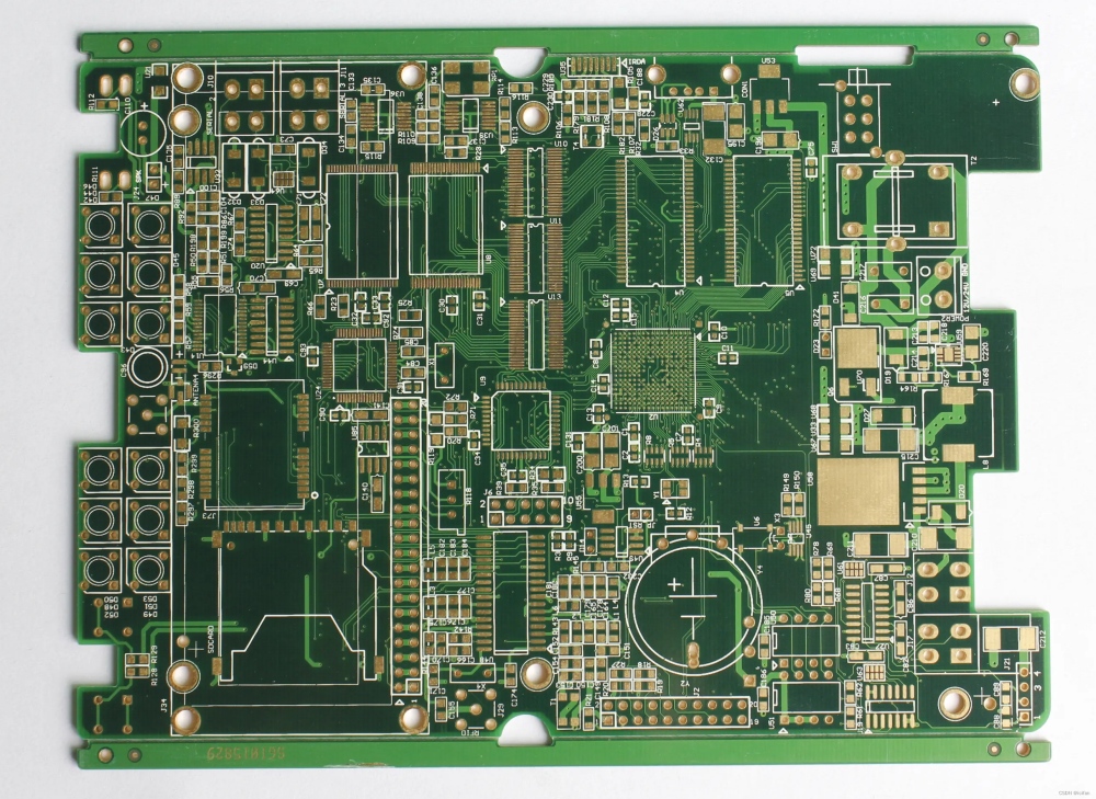
HDI (High Density Interconnect) boards are circuit boards with a high density of circuit traces, achieved through the use of micro-blind and buried via technology. HDI boards consist of inner and outer layers. We use processes such as drilling and via plating to connect the traces between these layers.
What are the fundamental differences between HDI and a standard PCB?
To understand how many layers an HDI PCB has, we must first clarify the fundamental differences between HDI PCBs and standard multilayer PCBs. In standard multilayer PCBs, such as common 4-layer or 6-layer boards, interlayer interconnection primarily relies on mechanical drilling (commonly known as through-holes). We typically control the diameter of these through-holes between 0.2 mm and 0.3 mm. We also keep a proper safety margin between holes, which restricts circuit layout density.
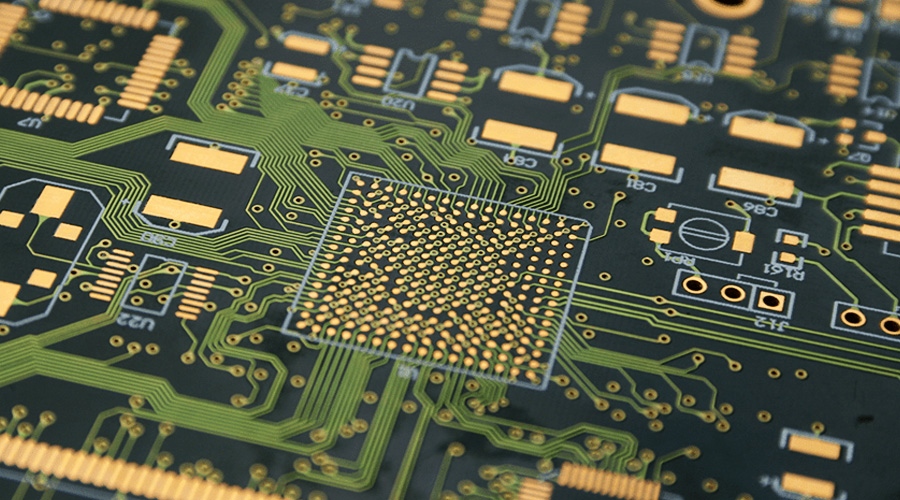
The core feature of HDI PCBs lies in their extensive use of laser drilling technology to create microvias. These microvias can have diameters as small as 0.1 mm or even less than 0.075 mm, and they can be blind vias or buried vias—meaning they do not need to penetrate the entire board as through-holes do. As a result, the space previously occupied by through-holes is freed up, allowing for the routing of more numerous and denser traces, thereby achieving higher routing density.
We therefore call this technology “High-Density Interconnect”, or HDI. We typically set the line width and spacing of standard PCBs from 0.15 mm to 0.2 mm. By contrast, we can produce HDI PCBs with line width and spacing as small as 0.075 mm or even 0.05 mm, and we can shrink pad diameters to below 0.2 mm. It is precisely these comprehensive improvements in technical specifications that enable HDI PCBs to achieve interconnect densities several or even dozens of times higher than standard PCBs on boards of the same size.
Structural Types of HDI PCBs
HDI boards can be classified into the following types based on the construction method of blind vias:
- Single-layer (1st-order HDI): The most basic HDI structure: core board + two blind via layers on both sides, commonly used in mid-range smartphones and consumer electronics.
- We add an extra blind via layer to the 1st-order structure to produce two-layer HDI (2nd-order HDI). We can arrange blind vias in an interlaced or stacked design, so this type suits flagship smartphones and tablets.
- Any-Layer HDI: Any two layers can be interconnected, and blind vias can be created between any layers, achieving extreme interconnect density. Suitable for high-end chip modules (such as Apple’s A-series packaging).
With the increase in layer count and the maturation of stacking technology, HDI boards have become the precursor structure for System-in-Package (SiP) and chip packaging substrates.
Challenges in HDI PCB Manufacturing
The manufacturing of HDI boards is far more complex than that of standard PCBs, with the main challenges lying in the following areas:
- High precision requirements for laser drilling and blind via alignment
Laser-drilled holes are small, with positional accuracy required within ±25 μm, placing extremely high demands on equipment capabilities and material stability. - Difficulty in controlling resin via filling and copper surface flatness
After blind vias are filled with resin, the copper surface must remain smooth and flat; improper handling can lead to poor soldering of surface-mount components. - High technical barriers for multiple lamination and layer alignment
The risk of interlayer misalignment is high during multiple lamination processes, necessitating the use of Automated Optical Inspection (AOI) systems and laser drilling positioning systems. - High circuit density and difficult electrical testing
Test probes struggle to make contact with minute pads, and impedance control and signal integrity simulation must be completed in advance.
Consequently, HDI board manufacturers typically possess exceptional engineering capabilities and high-end production equipment, positioning them as the “top tier” players in the PCB industry.
Future Trends in HDI PCBs
Looking ahead, HDI PCB technology will continue to evolve toward higher layer counts, finer traces, and lower costs. In terms of layer count, as chip packaging becomes increasingly complex and the number of pins continues to rise, 16-layer and even 20-layer or higher HDI boards will become increasingly common. Regarding trace fineness, the mSAP process is approaching the limit of 0.025 mm line width and spacing, which will enable PCBs to support higher-performance chips.
In terms of materials, high-frequency, high-speed materials (such as the Megtron and Tachyon series) are seeing increasingly widespread adoption. These materials feature lower dielectric constants and lower loss, better supporting 5G and 6G communications. In terms of costs, as we localize laser drilling equipment and refine the mSAP process, we gradually lower manufacturing costs for HDI PCBs. We expect to apply HDI PCBs from high-end products to mid-range consumer electronics in the future. In addition, we combine HDI technology closely with flexible substrates (FPC) and rigid substrates to produce rigid-flex PCBs.
These boards enable interconnections in three-dimensional space and represent a core technology for future foldable smartphones and irregularly shaped electronic devices.
How to Select the Appropriate Layer Count for HDI PCBs
For engineers and procurement personnel, selecting the appropriate number of layers for an HDI PCB requires a comprehensive consideration of multiple factors.
- First, consider the number of pins and the package type of the chip. We typically adopt 6-layer second-order HDI boards for BGA packages with over 500 pins.
- Second, consider the signal speed. We recommend using HDI boards with 8 or more layers for designs with high-speed signals like DDR4, PCIe, and USB 3.1 to guarantee signal integrity.
- Third, designers must consider spatial constraints. For compact boards with complex functions, you can adopt 10-layer or higher HDI boards to maximize space utilization.
- Finally, cost considerations are essential. While meeting performance requirements, it is advisable to choose a design with fewer layers to control costs.
In practice, a 6-layer HDI board is often the most cost-effective choice, as it meets the needs of the vast majority of consumer electronics products without incurring high costs.
Summary
In summary, HDI PCB is not defined by a fixed number of layers, rather, it is a PCB technology system centered on high-density interconnects. Boards ranging from 2 to over 20 layers can be classified as HDI PCBs, provided they incorporate core technologies such as laser microvias, fine traces, and high-density pads.
In practical applications, 4- to 10-layer boards are the most common choices, with 6-layer and 8-layer HDI second-order boards dominating the market. With the rapid development of technologies such as 5G, AI, and the Internet of Things (IoT), the number of layers in HDI PCBs will continue to increase, and the technology will continue to advance. Understanding the logic behind HDI PCB layer counts is of great practical significance for electronic engineers in product design and selection, as well as for procurement personnel in supply chain management.


