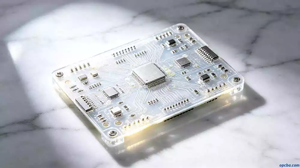
When you first pick up a transparent PCB sample, your immediate reaction is often, “That looks stunning”—the circuitry is clearly visible against the translucent substrate, much cleaner than the traditional green solder mask on FR‑4. But as soon as you start surface‑mount assembly and soldering, the problems appear: if your soldering iron is even slightly too hot, the edge of the board yellows; switch to a low‑temperature solder, and its poor flow leaves several “solder blobs” on the board.
This is not a skill issue—it’s because surface‑mount soldering on transparent PCBs requires a completely different approach from conventional PCB assembly. Starting from the material properties, this article breaks down the easily overlooked details throughout the entire process, from paste selection and reflow profiling to hand soldering and inspection. If you’re new to core printed circuit board fundamentals and basic terminology, start with our foundational overview: Printed Circuit Board(PCB)
1. Why Is Surface‑Mount Soldering on Transparent PCBs So Challenging? – First, Understand the Material’s Character
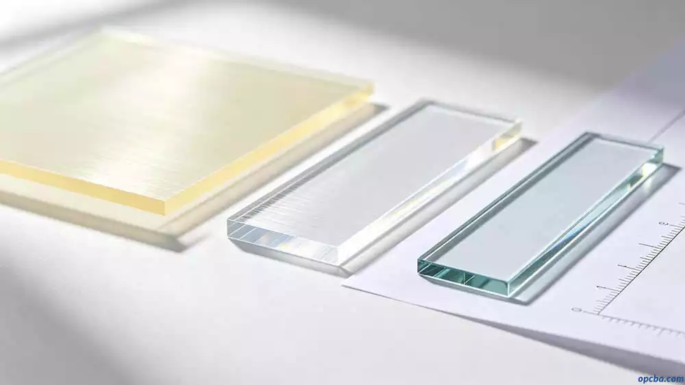
Surface‑mount soldering on transparent PCBs is challenging because the substrate is changed from FR‑4’s epoxy glass cloth to a highly translucent material. Most of what the market calls “transparent PCBs” are flexible circuits with a PET substrate, with light transmittance up to 85%–95%. A few use colorless polyimide (CPI) or glass substrates.
Soldering tolerance of the three substrate types:
| Substrate | Temperature Tolerance | Reflow Compatibility | Typical Applications |
|---|---|---|---|
| PET | ~150°C | Low‑temperature reflow only (<150°C) | Consumer electronics, disposable sensors |
| CPI | Tg typically 280–350°C; some high‑end grades can exceed 350°C | Can pass standard reflow | Transparent FPCs requiring high‑temperature reliability |
| Glass | High | Can pass standard reflow | Transparent display backplanes, photoelectric sensors |
The core difference from traditional FR‑4 is that FR‑4 can handle 260°C “like a walk in the park”—wave soldering and reflow are no problem. But PET‑based transparent PCBs are extremely temperature‑sensitive, with a very narrow soldering window. This is the starting point for all transparent PCB soldering work — temperature control is the first line of defence.
2. Pre‑Solder Preparation: Choosing the Right Materials Wins Half the Battle
How to choose solder paste – trade‑offs of low‑temperature alloys
For PET substrates, SMT assembly must use low‑temperature solder paste, commonly SnBi alloy (tin‑bismuth) with a melting point of about 138°C. But low‑temperature paste has a clear drawback: its flowability is worse than standard SAC305.
In practice, this means:
- Printing is more prone to insufficient paste or stringing.
- After reflow, solder joints are less smooth and have lower gloss.
- Mechanical strength of the joints is lower than SAC305.
A deadly hidden danger often ignored: SnBi alloy, when used long‑term in environments above 100°C, undergoes continuous bismuth phase coarsening, gradually embrittling the solder joints. This means that a product passing all tests at room temperature may develop cracked joints after months inside a sealed, high‑temperature chassis. If your product’s operating ambient temperature consistently exceeds 100°C, you must either switch to a CPI substrate with standard SAC305 paste, or consider using anisotropic conductive adhesive (ACA) instead of soldering. Actual reliability should always be verified with the specific alloy formulation and accelerated aging tests under your application conditions.
A common decision rule: If your product needs long‑term operation in high‑temperature environments, the PET + low‑temperature paste combination may not be reliable enough—either change to CPI substrate, or use conductive adhesives.
Stencil design adjustments
Because low‑temperature paste has poor flow, stencil apertures may need fine‑tuning. For fine‑pitch components of 0.5 mm and below, consider slightly reducing the aperture size to avoid excessive paste extrusion causing shorts. However, the exact adjustment depends on the actual paste type and the manufacturer’s process capability—there is no universal value.
Pad surface finish: OSP or ENIG?
For PET flexible transparent PCBs, OSP or ENIG is usually recommended for SMT soldering. Silver plating is not recommended because silver ions tend to migrate. OSP is cheaper but has a shorter shelf life and cannot withstand multiple reflow cycles; ENIG is more expensive but offers better solderability stability. If your transparent PCB requires multiple reworks or double‑sided assembly, ENIG is the more trouble‑free choice.
3. Reflow Profile: Don’t Treat PET Like FR‑4
This is the most common stumbling block in SMT on transparent boards.
Recommended approach for PET substrates: The reflow temperature must be kept below 150°C. Specifically:
- Peak temperature: 138–145°C (just above the SnBi paste melting point).
- Preheat zone: Ramp rate controlled at 1–2°C/s to avoid thermal shock.
- Time above liquidus (TAL): Recommended to be within 30–60 seconds. This is more critical than the peak temperature—even if the peak is not exceeded, a TAL of 90 seconds will still cause thermal accumulation that yellows the PET and reduces pad adhesion. When you have no existing empirical data, starting with 30–45 seconds and running a DOE verification is much safer than blindly copying the FR‑4 window of 60–90 seconds.
CPI and glass substrates are not so “delicate” and can follow standard lead‑free reflow profiles: preheat 150–200°C for 60–120 seconds, reflow peak 230–255°C.
A typical failure scenario: Engineers accustomed to FR‑4 profiles directly apply the same temperature curve to a PET transparent board. The result is yellowing, warpage, or even pad peeling after reflow. This often happens when a project switches from traditional boards to transparent boards without adjusting process parameters.
Why this happens: PET’s glass transition temperature is only about 80°C, meaning the substrate begins to soften above 80°C. The preheat zone of a standard reflow profile already far exceeds this—the substrate is essentially “baked soft then soldered” – deformation is inevitable. For a complete breakdown of standard SMT reflow and wave soldering processes and parameters for conventional boards, refer to our full guide: SMT Reflow & Wave Soldering for Lead-Free PCBA: Process Guide

4. Hand Soldering Transparent PCBs: The Pitfalls Nobody Tells You
Many R&D prototyping scenarios do not use stencils and reflow, but instead hand‑solder. At this point, the considerations for transparent PCB soldering are different again.
Iron temperature and solder wire selection: If hand‑soldering a PET transparent board, keep the iron temperature below 260°C (ideally 220–250°C) and use low‑temperature solder wire. One user shared a real experience: “With a normal iron, the board edge yellowed as soon as the temperature was a little high—I quickly switched to low‑temperature solder.”
Why transparent boards are more prone to “blobs”: Low‑temperature solder has poor flow, so during hand soldering it does not spread easily and tends to pile up as “solder blobs” on the pad. This is not a skill issue but a physical property of the material. Solutions: Slightly increase the iron dwell time on the pad (but be careful not to burn the substrate), or use additional flux to improve wetting.
Fatal risk during rework: Transparent substrates are much softer than FR‑4. One engineer reported: “As soon as I heated with a solder sucker, the substrate stuck a small piece onto the tip, ruining a perfectly good board.” For reworking transparent PCBs, it is recommended to heat from the back side with a hot‑air gun rather than contacting the pads directly with a desoldering tool.
5. Post‑Solder Inspection: The “Visual Trap” of Transparency
Transparent substrates present a special problem during inspection: surface defects are more conspicuous on a transparent board than on a green one.
Minor blemishes that would be insignificant on a green solder‑masked board may directly appear as visible artefacts on a transparent electronic product—reducing light transmittance or increasing haze. This means that transparent PCB quality standards cannot simply be copied from traditional PCBs.
AOI lighting adjustments: Traditional AOI equipment lighting is optimised for opaque PCBs. A transparent substrate changes light transmission and reflection, potentially increasing false‑call rates. In practice, you may need to adjust the lighting angle or intensity, or use backlighting.
Issues easily missed during visual inspection: Transparency makes the circuitry clearly visible, but it also makes flux residue around solder joints much more obvious. After soldering, thorough cleaning is mandatory; otherwise, residue will be very apparent on the transparent substrate and affect the product’s appearance.
6. Common Soldering Defects and Troubleshooting Logic (with Decision Branches)
| Defect Phenomenon | Possible Cause | Troubleshooting Order |
|---|---|---|
| Board edge yellowing / discoloration | Soldering temperature too high | ① Confirm substrate type ② Check iron / reflow temperature ③ Check if TAL exceeds limit |
| Solder “blobs” on pads | Poor flow of low‑temperature solder | ① Check paste type ② Adjust printing parameters ③ Add more flux |
| Tombstoning | Unsymmetrical pad design or uneven heating | ① Check pad symmetry ② Adjust reflow zone temperatures |
| Pad peeling | Substrate insufficient heat resistance or repeated heating | ① Confirm temperature not exceeded ② Reduce rework cycles |
| Substrate warpage after soldering | PET softened by heat | ① Lower peak temperature ② Shorten TAL to within 60 seconds |
| Solder joint cracking after long‑term use | SnBi alloy exposed to >100°C environment causing bismuth phase coarsening and embrittlement | ① Confirm actual operating ambient temperature ② If consistently >100°C, change to CPI substrate + SAC305 paste, or use ACA |
An important decision rule: When encountering soldering defects, do not rush to adjust equipment parameters. First confirm the substrate type—if it is PET, 90% of problems are due to excessive temperature. Reduce the temperature first, then consider other optimisations. And if the defect occurs at the customer site after months of operation, prioritise checking whether the ambient temperature has exceeded the reliable working range of the SnBi alloy.
7. Summary: Core Principles for Surface‑Mount Soldering on Transparent PCBs
Reviewing the entire article, the successful execution of surface‑mount soldering on transparent PCBs boils down to three core principles:
First, material dictates process. PET, CPI, and glass each have completely different soldering windows. When you receive a board, the first thing is to confirm the substrate type—do not directly apply empirical parameters from other boards.
Second, temperature is the biggest variable. For PET transparent boards, the soldering temperature must be strictly controlled below 150°C, and the time above liquidus (TAL) must be kept within the 30–60 second range—this is a prerequisite for all operations, with no exceptions.
Third, accept that “different” is normal. The gloss, flow, and mechanical strength of transparent board solder joints differ from those of traditional PCBs. This is not a quality issue—it is a material characteristic. Trying to apply FR‑4 standards to PET transparent boards will only trap you in endless rework cycles. If your product’s ambient temperature exceeds 100°C for extended periods, choose a CPI substrate from the start rather than struggling with low‑temperature paste on PET.
Transparent PCBs are indeed beautiful, but beauty depends on “good soldering.” We hope this guide on surface‑mount soldering on transparent PCBs helps you avoid a few pitfalls.