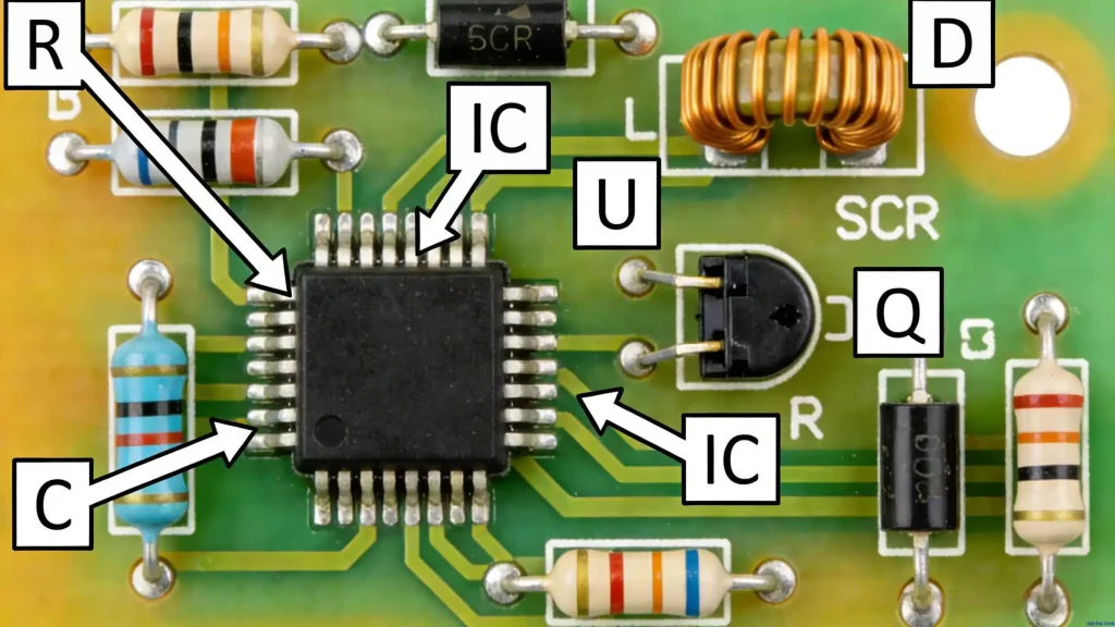
PCB Soldering Techniques
I. Core Process Flow of Selective Soldering
The standardized selective soldering process consists of four main steps: precise flux spraying, PCB preheating, local dip soldering, and targeted drag soldering. Among these, flux application is the most critical step before soldering and directly determines solder joint quality.
During heating and post-soldering cooling, the flux must remain active. This prevents solder bridging and protects bare copper areas and pads from oxidation at high temperatures.
In industrial production, an XY servo robot handles flux spraying. The PCB moves at a steady speed under the spray nozzle, and the system applies flux only to the preset soldering areas. This ensures targeted and effective coverage.
II. Precision Control of Flux Application
For selective soldering after reflow (especially in microwave peak processes), high-precision flux spraying is key to quality control. The preferred method is micro-dot jetting spraying. This approach limits flux to the exact soldering spots and prevents contamination of non-soldering areas, keeping the board clean.
Process requirements state that the flux dot diameter must exceed 2mm. To fully cover the target pad, the spraying position must have a tolerance within ±0.5mm. This ensures complete flux coverage on each solder point and lays a solid foundation for reliable soldering.
III. Differences Between Selective Soldering and Wave Soldering
Comparing selective soldering with conventional wave soldering clearly shows its unique features and advantages:
- Wave soldering immerses the entire bottom side of the PCB in molten solder.
- Selective soldering only contacts specified areas with the solder wave, achieving localized soldering.
Since PCBs have low thermal conductivity, the localized heating of selective soldering does not spread heat widely. This prevents thermal damage to nearby components, non-soldered joints, and board areas, offering excellent thermal protection.
Flux application also differs significantly:
- Wave soldering requires coating the whole bottom side of the PCB.
- Selective soldering applies flux only to the targeted bottom-side pads, greatly reducing flux usage and minimizing residue.
In terms of application, selective soldering is a specialized precision process. It is only suitable for soldering through-hole components on PCBs. Mastering its principles, parameter settings, and equipment operation is essential for achieving high yield rates and stable production.
PCB Soldering Guidelines
To standardize the PCB soldering process, improve yield, and reduce defects like cold joints, shorts, and misplacement, we have compiled the following guidelines. They cover inspection, material preparation, operating procedures, component soldering tips, and post-soldering inspection and cleaning.
I. Board Inspection and Drawing Verification
Before soldering, inspect each bare PCB for visible defects. Check for open circuits, shorted traces, lifted pads, board damage, and solder mask irregularities. At the same time, compare the board against the schematic, silkscreen, and layout files. Verify that silkscreen markings, footprint positions, and pin definitions match the design. This prevents assembly errors caused by discrepancies between the drawing and the actual board.
II. Material Organization and Pre-Soldering Preparation
Before starting, verify all components, materials, and tools against a complete bill of materials. Sort components by package size and type to improve workflow efficiency. Implement a material check-off system. After soldering each component type, immediately confirm and mark them off the list to avoid missing, misplacing, or over-soldering parts.
Implement strict ESD control measures. Operators must wear grounded wrist straps to prevent electrostatic discharge from damaging sensitive devices like MOSFETs, ICs, and precision resistors. Inspect soldering equipment beforehand. Ensure the tip is clean, oxide-free, and free of residual solder and flux. For beginners and when soldering small packages like 0603, use a chisel tip. It provides better contact with the pad, ensures uniform heating, and reduces difficulty.
III. Proper Soldering Sequence
To avoid component blockage and operational interference, follow this sequence: solder small and low-profile SMD components first, then larger and taller through-hole parts. This prevents tall components from blocking access to nearby pads. As a priority, solder critical precision devices like ICs early in the process to ensure accurate placement and alignment.
IV. IC Soldering and Alignment
Before soldering any IC, double-check its orientation against the silkscreen. Polarity and pin-one location must be correct. On most PCBs, the silkscreen shows a rectangular pad, notch, or dot as the pin-one indicator.
Start by tack-soldering one pin on one side of the IC. Gently adjust the IC position until all pins align perfectly with the pads. Then solder the opposite corner pin to secure alignment. Verify that the IC sits flat on the pads with no shifting or lifting before soldering the remaining pins. This prevents misalignment, cold joints, and solder bridging.
V. Polarity for Resistors, Capacitors, and Diodes
Ceramic capacitors and most resistors are non-polarized — they have no polarity requirement. However, LEDs, tantalum capacitors, and electrolytic capacitors are polarized. You must observe correct polarity, or the component may burn out or cause circuit malfunction.
As a general rule, the end with a color band, marking line, or notch indicates the negative terminal. For chip LEDs, the light-emitting side often indicates polarity. On the diode silkscreen, a vertical line marks the cathode (negative). Always match these markings to the polarity symbols on the PCB.
VI. Crystal Oscillator Soldering
Passive crystal oscillators typically have two pins and are non-polarized — no direction requirement. Active crystal oscillators usually have four pins, each with a defined electrical function. Before soldering, confirm each pin’s function against the PCB pad assignments. Solder them in the correct positions to prevent oscillation failure or circuit malfunction.
VII. Through-Hole Component Soldering
For through-hole parts like power modules, you may trim and shape the leads to fit the pad spacing if needed. After placing the component, apply solder from the bottom side using a soldering iron. Allow the solder to flow through the hole, wetting both the pad and the lead to form a reliable joint on the top side.
Use just enough solder — the joint should show good wetting without excess buildup. Prioritize mechanical strength and reliable electrical connection.
VIII. Issue Logging and Continuous Improvement
Throughout the soldering process, document any PCB design or process issues. Record instances of component interference, improper pad sizing, footprint mismatches, or silkscreen errors. Maintain a log to support future PCB revisions, process improvements, and footprint corrections.
IX. Post-Soldering Inspection
After soldering, inspect every joint using a magnifying glass. Check for cold joints, false joints, solder bridges, solder balls, insufficient wetting, or any other defects. Ensure every joint meets quality standards and guarantees reliable electrical conductivity.
X. Final Board Cleaning
After inspection, clean the entire PCB using a specialized solvent like isopropyl alcohol. Remove all solder splashes, flux residue, dust, and other debris. This prevents metallic particles from causing shorts or leakage and improves overall board cleanliness and reliability.
Double-Sided PCB Soldering Methods
As electronic devices move toward lighter, smaller, more functional, and highly integrated designs, traditional single-sided PCBs can no longer meet the routing and performance needs of precision electronics. Double-sided PCBs have become the mainstream solution due to their ample routing space, high integration, and compact structure. This shift also drives PCB manufacturing toward thinner, finer, and higher-density processes.
Compared to single-sided boards, double-sided PCBs have conductive traces on both layers and plated through-holes for interconnection. The soldering process is more demanding and requires standardized procedures to ensure reliable dual-layer conduction and good yield.
I. Pre-Soldering Board Preparation (Through-Hole Reinforcement)
The key feature of double-sided PCBs is the plated through-hole that connects the top and bottom layers. To ensure stable interconnection and prevent open vias or poor contact, you must reinforce these holes before soldering.
For each plated through-hole, use a small wire to solder and bridge the hole, strengthening the connection between layers. After this reinforcement, trim any excess wire protrusions to remove sharp tips. This avoids scratches during handling and completes the basic board preparation.
II. Standardized Soldering Procedures for Double-Sided PCBs
1. Component Lead Forming
For all through-hole components that require lead bending, always shape the leads before insertion. Follow the dimensions given in the assembly drawing. Do not insert components with unformed leads.
For diodes, after forming, ensure the part number marking faces upward. The leads should be symmetrical and equal in length. This guarantees proper alignment and meets process standards.
2. Polarity and IC Placement
When inserting polarized components, strictly match their polarity to the silkscreen markings on the PCB. Avoid reverse or incorrect insertion.
For ICs and other critical devices, whether mounted vertically or horizontally, the component body must sit flat against the board after insertion. It should show no significant tilting, shifting, or floating. This ensures soldering accuracy and device stability.
3. Soldering Equipment Parameters
Double-sided PCB soldering requires specific tool settings. Use a temperature-controlled soldering iron rated at 25–40W. Set the tip temperature to approximately 242°C.
- Too high a temperature will oxidize and damage the tip coating, and may burn the PCB substrate or sensitive components.
- Too low a temperature causes poor wetting and incomplete melting, leading to cold or weak joints.
Limit each soldering point to 3–4 seconds. Prolonged heating can damage components and copper traces.
4. Soldering Sequence
To avoid interference, component blockage, and thermal damage, follow this sequence: solder low-profile and inner components first, then taller and outer components. This prevents large parts from blocking access to smaller ones.
Strictly control the heating time at each joint. Excessive heat can burn components, blister the board, lift copper pads, or break traces.
5. Fixture Support to Prevent Damage
Because double-sided boards require soldering on both sides, use a dedicated soldering jig or frame to support the board during the process. The jig lifts and holds the PCB securely, preventing the top-side soldering operation from pressing against or damaging components already mounted on the bottom side. This keeps all components intact and properly positioned.
6. Post-Soldering Inspection and Touch-Up
After completing all soldering, perform a full inspection. Check every position for missing parts, missed joints, wrong components, cold joints, solder bridges, and other defects. Confirm that all component placement and solder joints meet quality requirements.
Once inspection passes, trim any excess leads, remove solder splashes, and clean residual flux and debris from the board surface. Only after passing this final check should the board proceed to the next production step.
7. Overall Process Compliance
All soldering operations must follow industry standards and the product-specific process documentation. Control every step — from component preparation and insertion to soldering and inspection — to ensure electrical reliability, mechanical integrity, and consistent quality for double-sided PCBs.