Ask any PCB fabricator which process generates the most customer complaints, and the answer usually points straight to solder mask. It’s the outermost layer, the board’s “clothing”—so every chip, scratch, or misalignment screams at the eye before a single test probe lands. Getting the PCB soldermask process under control is as much about layout rules as it is about the printing and curing steps. The gaps between pads are especially prone to trouble, and that’s where solder mask sliver and solder mask bridge enter the conversation.
The Tiny Green Wall That Prevents a Short
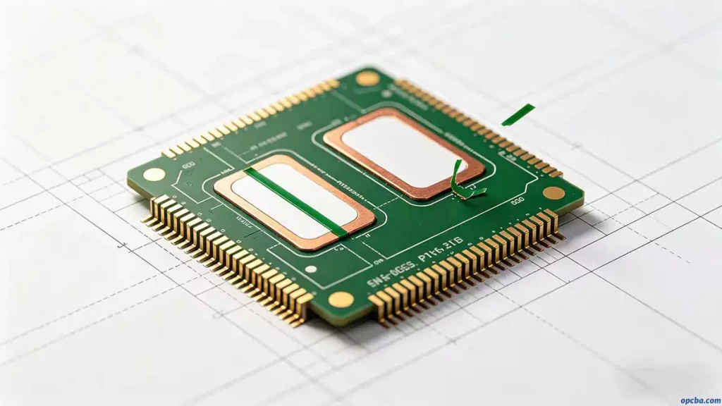
A solder mask bridge is the narrow strip of green ink left between two adjacent pad openings—most critical between the closely packed pins of an IC or connector. Its one job is to keep solder from riding across during reflow and creating a short. When that bridge is missing or too thin, you get a solder mask sliver: a thin, detached fleck of ink that can lift, fold over, or float away during processing. The result is exposed copper and, too often, a latent defect that field vibration turns into a hard failure. I’ve traced more intermittent shorts back to a lost solder mask sliver than I’d like to count.
Three design numbers set the stage:
- For 1 oz copper, keep the solder mask clearance gap at 0.08 mm (3 mil) or larger.
- The solder mask bridge width needs at least 0.10 mm (4 mil). If you’re using immersion tin (lm-Sn), bump that to 0.125 mm (5 mil); the chemical attack of the tin bath can weaken a thin bridge.
- The N-cap extension of the mask over a conductor should not drop below 0.08 mm (3 mil).
Exact minimums shift with copper weight, mask imaging method, and surface finish, so checking with the fab house early in the PCB soldermask process prevents heartburn later.
Via and BGA Mask Choices That Influence Yield
How you handle vias in the solder mask design changes assembly behavior. Through-holes can be plugged (half or full), left with a small opening, or opened fully. The right choice depends on whether paste will print over them and whether gas entrapment inside the hole is a risk. For BGA arrays, plugged vias under the chip prevent solder wicking down into the board and help keep pad coplanarity within spec. I’ve learned to default to via-in-pad plugged and capped when the pitch drops below 0.8 mm.
Troubleshooting Screen Room Headaches
Even with a solid solder mask design, the wet process on the factory floor can introduce its own issues. Below are the most common ones I’ve run into, boiled down from supplier feedback and my own board inspections.
- Bleeding / Blurring — Ink viscosity is too low, or the screen-to-board spacing is off. Raise the ink concentration and check the gap. Don’t just dump in thinner.
- Incomplete Curing — Oven exhaust might be clogged, the actual temperature may not match the setpoint, or the thinner used is the wrong speed or insufficiently dosed. Measure the oven profile before adjusting chemistry.
- Green Oil Bridge Broken — This often traces back to underexposure or poor surface preparation. Increase the exposure energy and verify that the pre-treatment line is running within spec. A broken solder mask bridge is as good as none: it invites solder splash into the next pad.
Every one of these defects shows up visually, which is why final optical inspection of the PCB soldermask process matters. Candids taken off the line might look fine, but a missing solder mask sliver at 50x magnification tells a different story. For a deeper dive into the full production workflow behind these steps, see our guide: Soldermask in PCB production


