Poor PCB panel design is a recipe for costly manufacturing disasters: warped boards, misplaced components, and assembly line stoppages. Whether you’re prototyping or scaling up, getting the panel right is non-negotiable for SMT compatibility and a smooth production flow.
A well-designed PCB panel not only improves PCB Assembly(PCBA) efficiency but also reduces waste and ensures consistent quality. Below, we break down the core rules, key design methods, and critical details (like mark points and positioning holes) you need to know.
Key PCB Panel Design Principles
Before diving into specific rules, start with these foundational principles to avoid common mistakes:
- Closed-Loop Border Design: For PCB panel borders (clamping edges), use a closed-loop design. This ensures the panel stays rigid and doesn’t deform when fixed in assembly fixtures—critical for maintaining precision during SMT placement.
- Square/Rectangular Shape: Design panels to be as close to square as possible. Preferred panel configurations include 2×2, 3×3, or other grid layouts (e.g., 2×3) to maximize material usage and simplify handling.
- Avoid Overcrowding: Ensure components (especially large or protruding ones) don’t interfere with panel borders, cutting paths, or fixture clamps—this prevents damage during assembly and separation.
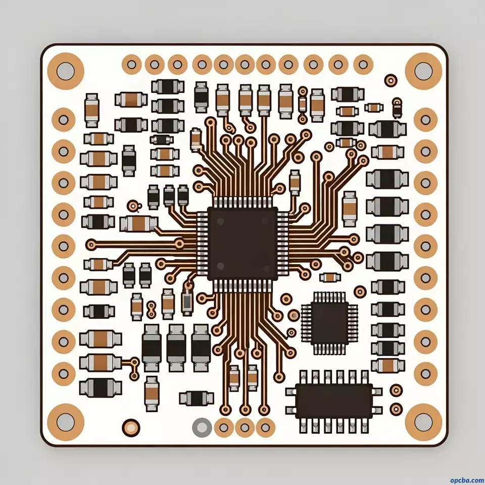
1. Guiding the Machine: Fiducial Mark Best Practices
Fiducials, or simply “marks,” are those little copper dots that act as optical reference points for SMT placement machines. Follow these best practices to ensure reliable positioning:
(1) Mark Point Size & Clearance
Ensure a clear, solder-mask-free zone around each fiducial (typically a 1.5mm radius from the mark’s edge) so the vision system can lock onto it reliably.
(2) Mark Point Placement
- For PCBs with SMD components, place at least two mark points at opposite corners of the panel (or individual board within the panel). This provides dual reference points for accurate optical positioning.
- For multi-layer PCBs, place mark points at the opposite corners of each layer to ensure alignment across layers during assembly.
(3) Mark Points for High-Precision Components
For components with tight spacing—such as QFP (Quad Flat Package) with lead spacing ≤0.5mm or BGA (Ball Grid Array) with ball spacing ≤0.8mm—add extra mark points at the two opposite corners of the IC. This enhances placement precision and reduces soldering defects (like bridging or misalignment).
In short, they are the alignment stars for the pick-and-place machine — without them, it’s flying blind. They ensure components are soldered in the exact right spot, even for the smallest parts.
2. Protecting the Perimeter: Process Edge Do’s and Don’ts
The process edge (also called the panel border) is the area of the panel used for clamping, handling, and cutting. Follow these guidelines to avoid assembly issues:
- No Protruding Components: Do not place large or protruding components along the panel border, between individual boards, or at board-to-board nodes. This prevents interference with SMT machine clamps and cutting tools.
- Clearance Requirement: Leave at least 0.5mm of empty space between all electronic components and the panel edge. This ensures cutting blades can operate normally without damaging components or PCB traces during panel separation.
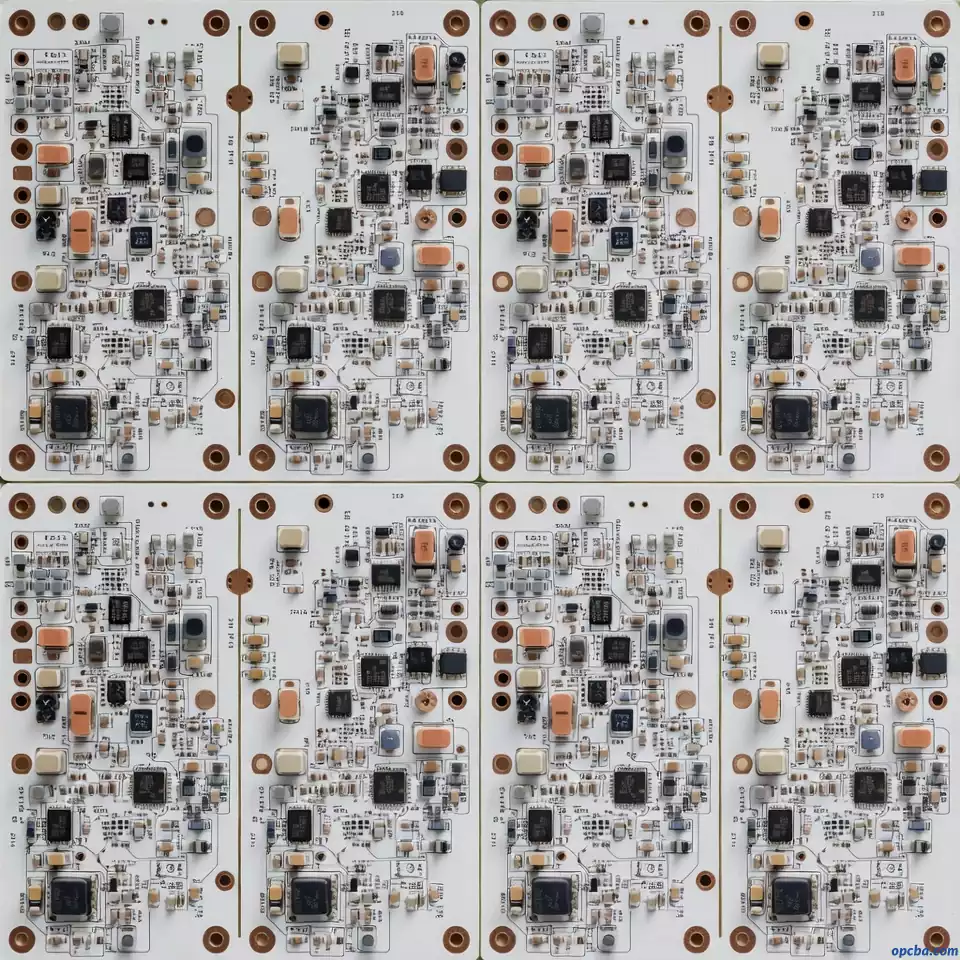
3. Locking It Down: Positioning Holes for Precision
Positioning holes are used for precise alignment of the panel during assembly, testing, and cutting. They are critical for maintaining accuracy, especially for fine-pitch components.
(1) Positioning Hole Placement
- For PCBs with fine-pitch components (e.g., QFP with lead spacing <0.65mm), the preferred practice is to ensure the board’s global fiducials and positioning holes are precise, and add local fiducials for the component (as noted earlier). Positioning holes primarily secure the board, while fiducials serve as the final reference for machine vision. If you do place positioning holes at the component’s opposite corners, this is typically an alternative or enhancement when local fiducials cannot be added, or for physical positioning during manual soldering — not a standard practice.
- For panel assembly (combining multiple PCBs into one panel), use paired positioning holes placed at the opposite corners of the panel. This provides stable alignment for the entire panel during SMT processing.
(2) Positioning for Large Components
For large or heavy components—such as I/O sockets, microphones, battery connectors, toggle switches, headphone jacks, or motors—add positioning columns or extra positioning holes. These prevent component movement during assembly and ensure mechanical stability in the final product.
Pro Tips for PCB Panel Design
- Test Panel Design First: Before mass production, create a test panel to verify mark point detectability, process edge clearance, and positioning hole alignment. This avoids costly mistakes in full-scale production.
- Consider Cutting Methods: If using V-scoring or routing for panel separation, design the panel with enough space for cutting tools (e.g., 0.8–1.0mm for V-scores).
- Align with SMT Machine Requirements: Check your SMT machine’s specifications for mark point size, positioning hole diameter, and panel size limits—this ensures compatibility.
Applying these rules correctly can be the difference between a smooth launch and a costly re-spin. If you need help with your panel layout, or want to learn more about One Stop PCB Assembly Services to streamline your production, the engineering team at OPCBA is a good place to start. You can find more resources and contact info at opcba.com.


