
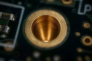
PCB: Plated Vias
Plated vias are one of those PCB processes we use all the time—but they’re easy to overlook until something goes wrong. Put […]
Etching, drilling, plating, lamination, surface finish, soldermask, warp control, production flow.
Plated vias are one of those PCB processes we use all the time—but they’re easy to overlook until something goes wrong. Put […]
Vias are among the most critical features in multilayer PCBs, and drilling costs typically make up 30% to 40% of total PCB
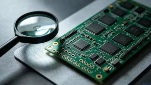
Through-holes connect different layers on a PCB and carry electrical signals between them. As electronics keep evolving, PCB fabrication and SMT assembly

Etching is the manufacturing step that removes unwanted copper from a circuit board to leave the traces, pads and planes the design
HASL remains one of the most widely used surface finishes in PCB production, and Lead-free HASL PCB has become the standard as

PCB copper plating quality directly impacts the board’s application reliability. As PCBs move toward higher density and precision, demands for plating quality

In automated surface mount lines, warped or non-flat circuit boards trigger a cascade of production issues. They cause inaccurate positioning, failed component
PCB etching technology is a core process in PCB fabrication, used to create precise circuit patterns on copper-clad substrates. It leverages the

In the PCB manufacturing industry, terms like “through via”, “blind via” and “buried via” are everywhere—especially in high-density board designs. PCB drilling
In the PCB FR-4 copper clad plate industry, the semi-solidified sheet is a key commodity—especially for multilayer PCB manufacturing. PCB FR-4 CCL
PCB surface treatments are critical for protecting copper traces, enhancing solderability, and ensuring reliable electrical connections in electronic devices. Choosing the right
The production process of rigid PCBs may vary slightly based on factors like layer count, design complexity, and performance requirements, but the
ENIG and HASL are the two most widely used PCB surface finishes, and choosing the wrong one can lead to direct, costly

To begin with, PCB side plating—also commonly referred to as edge plating—is a specialized PCB fabrication technique involving copper plating that extends

What Is PCB Board Warp & Its Related Damage First of all, PCB board warp refers to the bending or deformation of
sales@opcba.com