
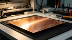
What is Copper Balancing?
Anyone who’s worked in PCB fabrication knows a well-made board isn’t just about following design files—it’s about nailing the small details that […]
Anyone who’s worked in PCB fabrication knows a well-made board isn’t just about following design files—it’s about nailing the small details that […]
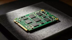
As electronics grow more advanced, assembly standards for printed circuit board assembly keep rising. The overall reliability of any electronic device ultimately
The green protective layer on finished PCBs is known as the PCB solder mask, a thin ink coating applied across most of
Two boards can run through the same etching line on the same day and come out at different quality. The difference nearly
PCBs built for harsh, extreme environments must perform reliably under punishing conditions: extreme temperature swings, high humidity, constant vibration, severe shock, and
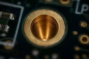
Plated vias are one of those PCB processes we use all the time—but they’re easy to overlook until something goes wrong. Put
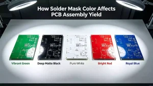
If you’ve handled PCBs long enough, you’ll notice one thing pretty quickly: most boards are green. Not because engineers care about the
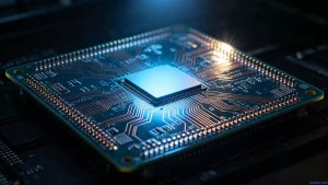
IC carrier board — also called a packaging substrate — is essentially a high-end PCB that acts as the signal bridge between
High-speed electronic designs rely on stable signal transmission, and trace impedance management sits at the core of reliable performance. On standard circuit
If you work with consumer electronics—cell phones, notebooks, digital cameras—you’ve probably handled FPCB without realizing it. Short for flexible printed circuit board
In our daily PCB assembly and maintenance work, we often see new technicians struggle with component identification. It’s a foundational skill—after all,
Every integrated circuit is built to deliver consistent electrical functions, and even minor physical defects during production can make a chip unusable.
When designing portable electronics or compact devices, we often get asked: what’s the difference between FFC and FPC connectors? Which one should

Vias are among the most critical features in multilayer PCBs, and drilling costs typically make up 30% to 40% of total PCB
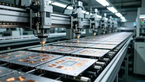
Most engineers reach for a heatsink the moment a component runs warm. The reflex is understandable, but a finned sink is not
In PCBA (Printed Circuit Board Assembly) processing, soldering defects are one of the most common issues we face. Among them, false soldering
What Copper Clad PCB Means A bare board layout usually shows large solid areas of blue or red in the EDA tool.
sales@opcba.com