Why the Soldermask of PCB Is Really Important
A proper PCB soldermask coating solves many common circuit board issues that designers and manufacturers face every day. Its most basic job […]
A proper PCB soldermask coating solves many common circuit board issues that designers and manufacturers face every day. Its most basic job […]
If you work with consumer electronics—cell phones, notebooks, digital cameras—you’ve probably handled FPCB without realizing it. Short for flexible printed circuit board
In real PCB production, traditional methods mean expensive molds, long lead times, and high setup costs—especially for small batches or prototypes. This
Electronics are everywhere in 21st-century life—from our phones to our home appliances. But have you ever wondered what’s inside those devices, and
Every month, we work with dozens of LED lamp manufacturers—and one question comes up time and again: what’s the best PCB material
In the fast-evolving electronics industry, thermal management and structural reliability have become major challenges for high-power circuits. This real demand led to
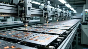
Anyone who’s worked in PCB manufacturing knows that turning a blank copper-clad board into a usable circuit isn’t just about machinery—it’s about
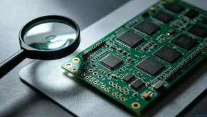
Anyone who’s worked in PCB fabrication knows a well-made board isn’t just about following design files—it’s about nailing the small details that
The green protective layer on finished PCBs is known as the PCB solder mask, a thin ink coating applied across most of
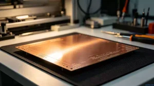
PCB etching is the step that transforms bare copper-clad boards into functional circuits, by chemically removing unprotected copper to leave only the
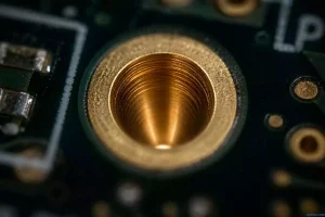
Plated vias are one of those PCB processes we use all the time—but they’re easy to overlook until something goes wrong. Put
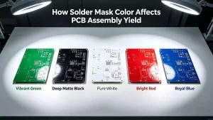
If you’ve handled PCBs long enough, you’ll notice one thing pretty quickly—most boards are green. Not because engineers care about the color,
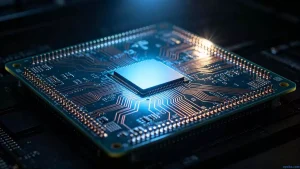
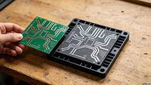
IC carrier board — also called a packaging substrate — is essentially a high-end PCB that acts as the signal bridge between
High-speed electronic designs rely on stable signal transmission, and trace impedance management sits at the core of reliable performance. On standard circuit
For LED drivers and high-power integrated circuits, heat buildup is one of the biggest threats to performance and lifespan. This is exactly
Vias are among the most critical features in multilayer PCBs, and drilling costs typically make up 30% to 40% of total PCB
Through-holes connect different layers on a PCB and carry electrical signals between them. As electronics keep evolving, PCB fabrication and SMT assembly
sales@opcba.com